Effective PCB Power Distribution Network Design
Key Takeaways
-
Key factors like vias, return paths, controlled impedance, and plane layer management are critical to PDN effectiveness.
-
Using tools like Allegro X can optimize PDN design, offering features such as real-time design rule checks and power plane generation.
-
Ensuring symmetry in board layer stackups and checking with manufacturers can prevent issues like board warpage and soldering defects.
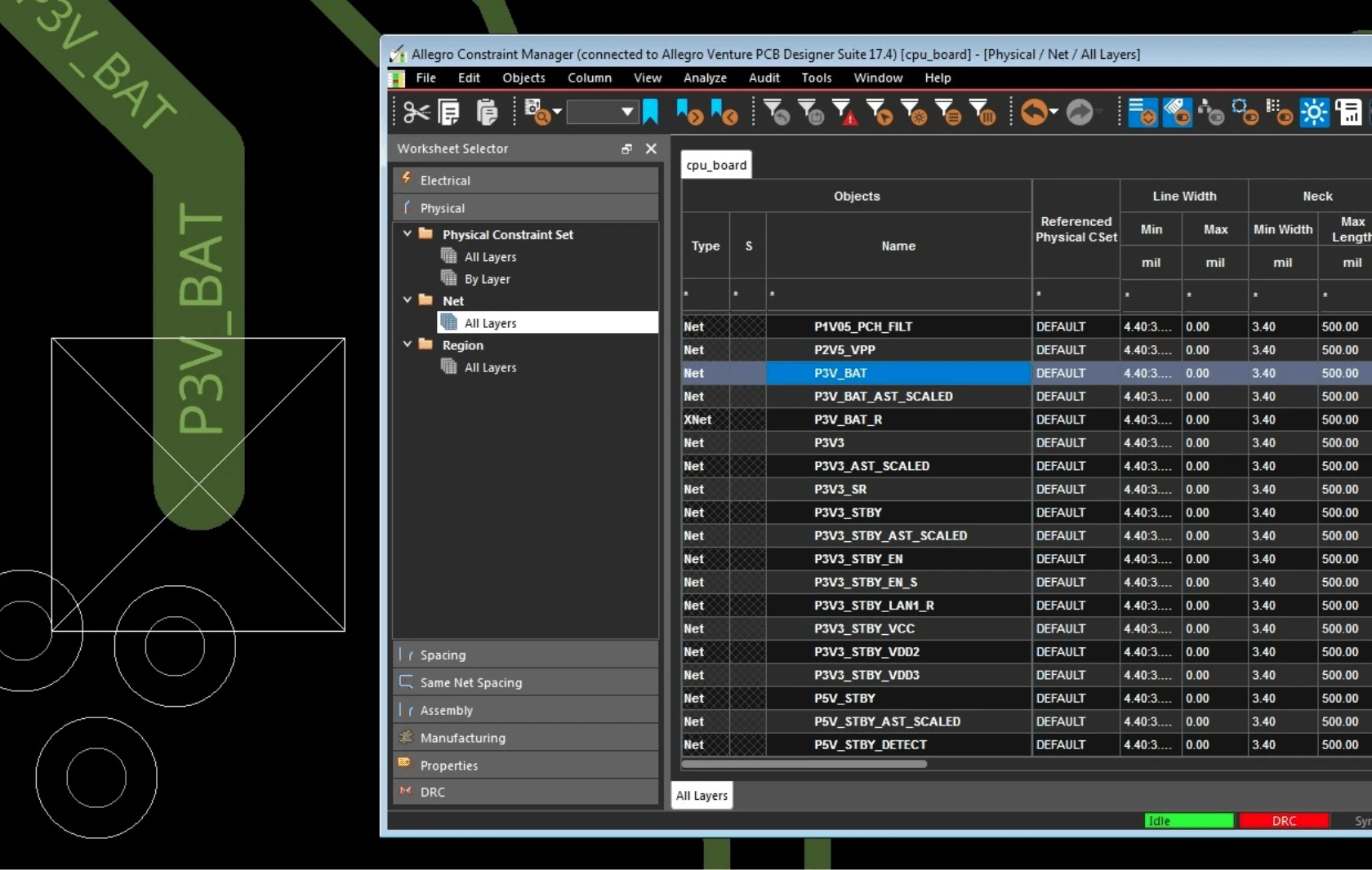
Using a design rules and constraint manager to set up the routing width of a PDN net.
A PCB power distribution network (PDN) ensures power is delivered efficiently to components in a board while maintaining stable voltage levels and minimizing noise. For example:
- In smartphones, the PDN distributes power from the battery to the CPU, GPU, memory modules (RAM and flash storage), and the display.
- In data centers, PDNs distribute power across servers and networking equipment, including CPUs GPUs, memory DRAM, storage devices (SSDs and HDDs), and networking components (switches and routers).
- In modern vehicles, PDNs distribute power from the car's battery to the engine control unit (ECU), infotainment systems, advanced driver-assistance systems (ADAS), and sensors.
To create such a PDN, using a power distribution network design tool is necessary –read on as we discuss PDNs and how such a tool can aid in design.
How PCB Power Distribution Network Manages Power and Ground
In the past, PCBs only had a single power and ground pin that could be easily connected with a simple wide trace. Then, as circuit density grew, it became easier to connect them with power and ground planes in a multi-layer board. But as pin-counts rose and the power requirements of ICs got more complex, circuit boards started experiencing some problems, requiring a power distribution network for smooth operation.
Key Considerations for PCB Power Distribution Network (PDN) Design
|
Aspect |
Key Points |
|
Vias and Return Paths |
- High-density parts require many vias, filling planes. |
|
Controlled Impedance Routing |
- Ground planes provide microstrip or stripline layer configurations. |
|
Plane Layer Management |
- Even distribution of power and ground nets is crucial. |
|
Ground Bounce |
- Simultaneous switching of digital signals can cause ground bounce. |
|
Power Ripples |
- Power supply switching can create noise or ripples. |
Along with the faster switching speeds of modern circuitry, there are many more power and ground connections on an IC that have to be managed. With a large processor chip in a ball-grid array (BGA) package, there can be hundreds of power and ground pins at various reference levels. These pins can also pull a lot of current to power the processor, and making sure that the power is clean without any spikes, ripples, or noise requires a carefully designed PDN.
Allegro X As A Power Distribution Network Design Tool
With all the different design requirements associated with creating a good PDN, it is helpful to have a good power distribution network design tool that can handle rules and constraint management systems. As you can see in the picture below, Allegro X PCB Editor has a power delivery generator, where you can set up your power and ground nets with the width and spacing rules that you need for your power net classifications.
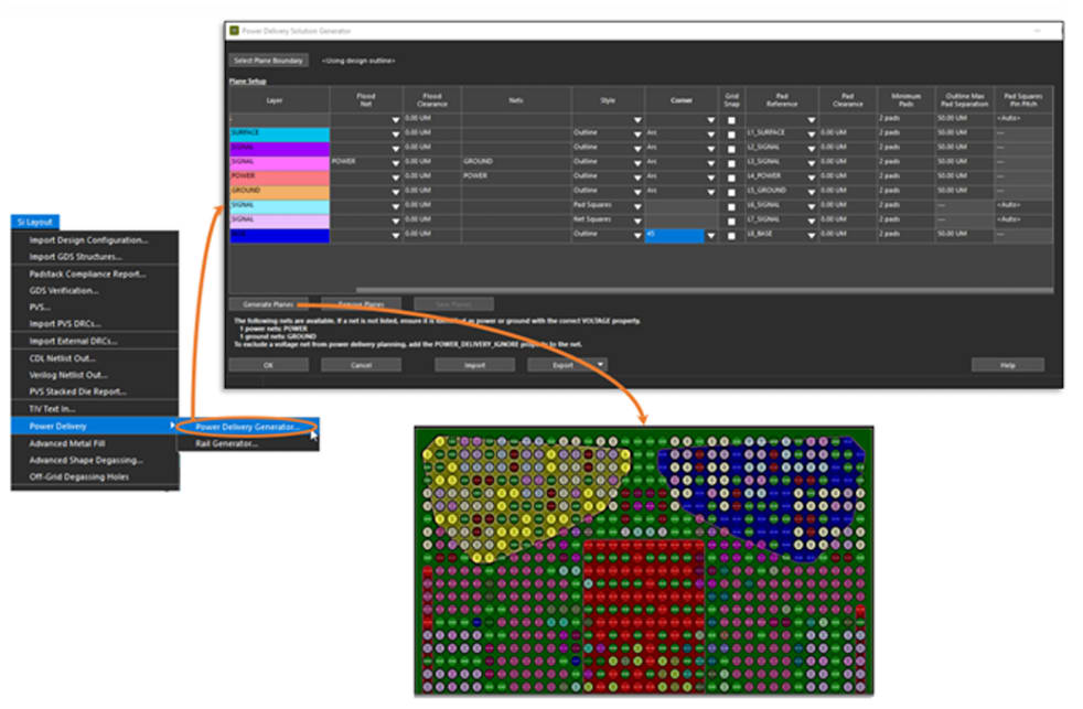
The Power Delivery Plane Generator creates power and ground planes based on pin or via locations within the target area.
Allegro X is a powerful tool for designing efficient PCB power distribution networks. Leveraging advanced AI and real-time design rule checks, Allegro X acts as a power distribution network design tool by integrating features such as the Power Plane Generator, which automates the creation of power and ground planes based on pin locations.
Allegro X Features for PDN Design
|
Feature |
Description |
Usage in PDN Design |
|
Power Plane Generator |
Automates the creation of power and ground planes by identifying clusters of pins or vias and generating plane boundaries. |
Simplifies the layout of power distribution networks by automatically generating planes, ensuring efficient power delivery. |
|
Real-Time Design Rule Check |
Provides interactive 3D feedback and instant design rule checking, identifying issues such as impedance mismatches and IR drop early in the design process. |
Enables immediate identification and resolution of power integrity issues, ensuring reliable power delivery across the PCB. |
|
Transmission Line Calculators |
Calculates stack-up material properties and trace dimensions to meet design requirements, ensuring optimal signal and power integrity. |
Ensures that power traces and planes are designed to handle the required power levels without causing signal degradation. |
|
DesignTrue DFM |
Integrates manufacturer-specific constraints into the design process, ensuring that the design meets fabrication, assembly, and test requirements. |
Ensures that the PDN design is manufacturable and free from errors that could compromise power delivery performance. |
|
Fill-In Material Specification |
Allows the specification of fill-in materials for conductor or plane layers, providing more realistic simulation results. |
Enhances the accuracy of thermal and electrical simulations, leading to better PDN performance. |
|
Sigrity X Integration |
Integrated with Sigrity X technology for advanced analysis of high-speed signals and power delivery networks. |
Facilitates the optimization of PDN design by providing detailed analysis and feedback on signal and power integrity. |
|
DFM Wizard |
Aids in setting up design rules based on IPC standards, ensuring compliance with manufacturing requirements during the design process. |
Helps in configuring design rules that directly impact the manufacturability and reliability of the PDN. |
|
IR Drop Vision |
Integrated analysis tool available in Allegro X PCB Editor that shows power integrity status in real-time, highlighting pins not receiving sufficient voltage. |
Allows for immediate corrections to power nets, ensuring all components receive adequate voltage, enhancing PDN reliability. |
The platform's comprehensive design checks and analysis workflows such as impedance and IR drop, ensure that engineers can identify and resolve potential issues early, reducing post-analysis rework. With its ability to perform thermal and electrical performance analysis, Allegro X allows designers to achieve first-pass manufacturing success by adhering to manufacturer-specific constraints. You can find out more information on how to create an effective PDN by looking at this E-book.
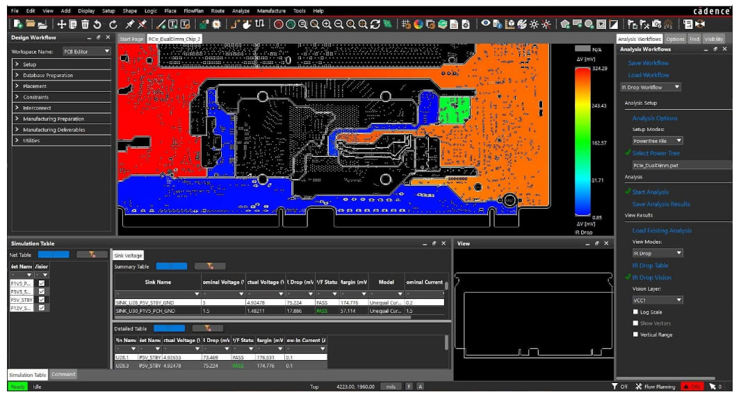
Analysis workflows such as IR Drop in Cadence Allegro X can help plan out an effective PDN.
PCB Manufacturing: Another Aspect of Your PDN Design Guide
Although a good PDN design may require the use of a non-symmetrical board layer stackup, some manufacturers will have a problem with that configuration. PCB fabricators usually prefer for the top layers of the board layer stackup to be mirrored in the bottom layers to create a symmetrical layer stackup.
With the temperatures and high pressures of the fabrication process, the combination of an uneven layer stackup can lead to warpage of the board. The larger the board, the more pronounced this effect can be. Board warpage can put stress on the thin metal traces used in long, high-speed transmission line routing, as well as on solder joints. To avoid these problems, circuit board designers should consider the following:
- Keep the power and ground plane layers symmetrical in the board layer stackup without compromising signal integrity.
- Make sure that the prepreg and core layers are also symmetrical in their thickness throughout the board layer stackup.
- Keep the densest copper layers of the board in the center of the stackup. Again, this has to be done in conjunction with good signal integrity practices.
- Use the same copper weight for the different plane layers.
- Consider adding metal fills (copper pours) in areas of the board that don’t already have much metal on them.
- Most importantly, check with your PCB manufacturer on your proposed board layer stackup before you commit to it to ensure that they will be able to fabricate it.
There is a lot to know about designing a good PCB power distribution network on your circuit board, and fortunately, your design tools provide plenty of help. With Cadence power distribution network design tools, such as Allegro X, designers can streamline the PDN design process. To learn more about how Cadence's PCB Design and Analysis Software can enhance your designs, visit the PCB Design and Analysis Software page. For more specific details on Allegro X, check out the product page.
Leading electronics providers rely on Cadence products to optimize power, space, and energy needs for a wide variety of market applications. To learn more about our innovative solutions, talk to our team of experts or subscribe to our YouTube channel.