Layout the Hot Loop, Save the EMI: Practical Allegro X Constraints for SMPS
Every switch-mode power supply has a noise source built in. It's not a bug-it's the topology. Fast-switching currents create fast-changing magnetic fields, and fast-changing magnetic fields radiate.
The question isn't whether your flyback will generate EMI. The question is whether you control it at the source or fight it everywhere else.
If you want a deeper understanding of why hot loop layout is so critical in switching power supplies, this on-demand webinar on the physics-based foundations of power supply design explains how switching behavior, field interactions, and energy flow create the EMI that layout techniques aim to minimize.
For a 5V/2A USB-C adapter, passing EMI certification isn't optional. FCC, CE, and other regulatory bodies require conducted and radiated emissions below specified limits. Fail the test, and you don't ship.
The good news: most EMI problems trace back to one thing. The hot loop. Get it right in layout, and compliance becomes manageable. Get it wrong, and no amount of filtering will save you.
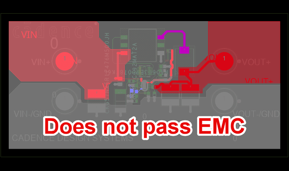
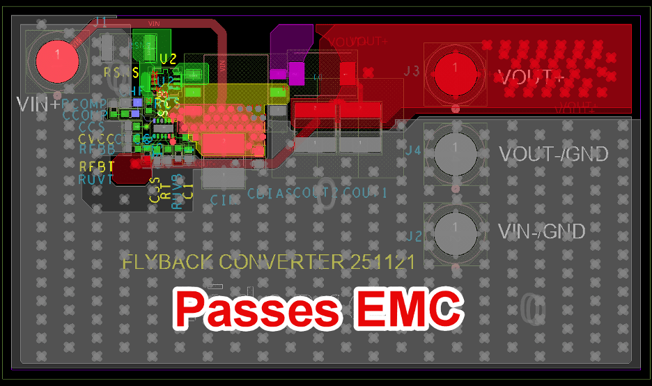
Same Electronics. Two PCB layouts-same design, different hot loop layouts. One passing, one failing.
What the Hot Loop Is (Physically)
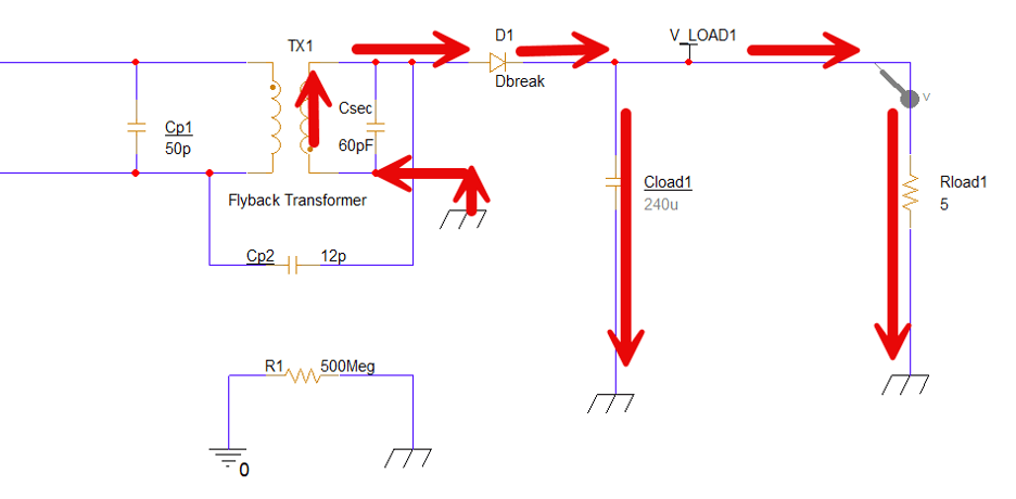
The hot loop is the path where current changes fastest. In a flyback primary side, it's the route from:
- Input bulk capacitor positive terminal →
- MOSFET drain →
- Transformer primary winding →
- Back to bulk capacitor negative terminal (ground)
When the MOSFET turns on, current rushes through this path. The transition takes 10-20 nanoseconds. That's fast enough that the loop acts as a transmitting antenna.
The radiation intensity is proportional to the loop area. Bigger loop = more radiation = harder to pass EMI.
For a 10W adapter, shrinking the hot loop from 200mm² to 50mm² can mean the difference between passing radiated emissions with margin and failing by 10dB.
The Three Rules
Rule 1: Place Hot Loop Components First
Before connectors. Before control circuitry. Before you think about mechanical constraints. Place the hot loop components first.
The sequence I follow:
- Input bulk capacitor - This is the energy reservoir. It anchors one corner of the loop.
- MOSFET - Position for minimum distance to the capacitor's positive terminal.
- Transformer - Orient so the primary pins face the switch, not away from it.
- Gate driver components - Cluster near the MOSFET to minimize gate loop inductance.
Everything else-controller IC, feedback network, output capacitors-works around these four elements. They're flexible. The hot loop is not.
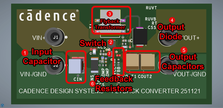
Step-by-step placement sequence of major components for a Flyback Converter.
Rule 2: Route Wide, Short, Single-Layer
Once placed, the route should be almost obvious:
- Wide traces: Use the widest your design rules allow. For the high-current paths, 40-60 mils minimum. Wider traces have lower inductance and lower resistance.
- Short paths: Direct point-to-point. Every millimeter of trace adds inductance. At 20ns switching edges, a few nanohenries of extra inductance creates measurable voltage spikes.
- Single layer: Keep the entire hot loop on one layer if possible. Each via adds roughly 0.5-1nH of inductance. Three unnecessary vias in the hot loop can add 2-3nH-enough to affect your EMI signature.
- Continuous ground plane underneath: The return current wants to flow directly under the forward current path. That's the lowest inductance route. Any gap in the ground plane forces a detour, which increases effective loop area.
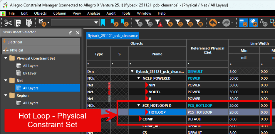
Rule 3: Encode Constraints So You Don't Forget
Rules 1 and 2 require discipline. But discipline fails at 4pm on Friday when you're trying to finish the layout.
This is where Allegro X constraints come in. You can encode your intentions as design rules:
- Minimum trace width for power nets: Set the MOSFET drain and transformer primary nets to require 50 mil minimum width. If you accidentally route them narrower, DRC flags it.
- Net class spacing: Create a net class for the hot loop nets with tighter spacing requirements. Keeps them close together during routing.
- Layer restrictions: Constrain the hot loop nets to specific layers (e.g., top layer only). Prevents accidental via transitions.
- Region keep-outs: Define a keep-out region that prevents other components from landing in the hot loop area. Protects the placement you carefully optimized.
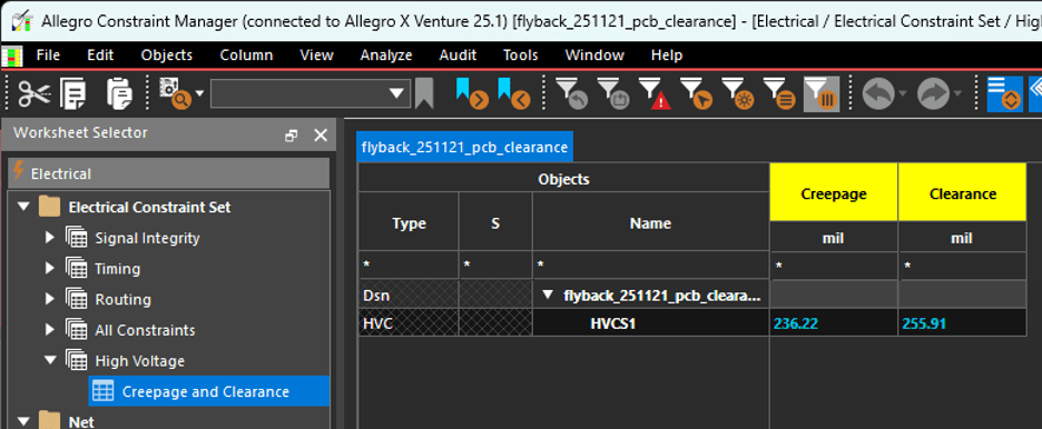
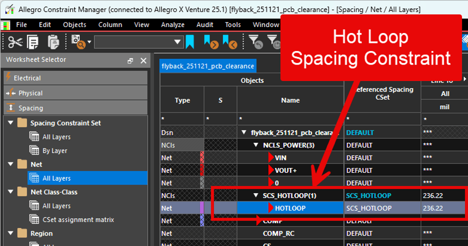
Allegro X Constraint Manager screenshot showing net class definitions for hot loop nets. Trace width and spacing constraints.
Secondary Hot Loop
The primary-side hot loop gets most of the attention, but there's a secondary-side hot loop too:
Flyback Secondary Side Current flow: Output rectifier cathode → Output capacitor positive → Transformer secondary → Output rectifier anode
This loop also carries fast-changing current (during the flyback phase when the secondary diode conducts). It's typically less violent than the primary loop because the currents are higher but the di/dt is lower, but it still matters.
The same rules apply: minimize area, use wide traces, keep a solid ground plane underneath.
For a 5V/2A output, the secondary loop carries up to 2A with transitions of maybe 50-100ns. Less aggressive than the primary, but still worth optimizing.
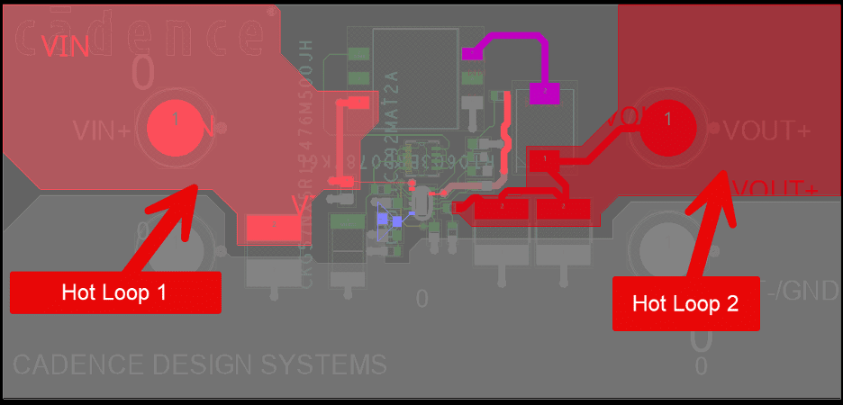
PCB layout showing both primary and secondary hot loops highlighted in different colors.
Ground Plane Continuity
I've said "continuous ground plane" several times. Here's why it matters:
High-frequency return current takes the path of lowest inductance. That path is directly underneath the forward current trace, as close to it as the stackup allows.
If there's a gap in the ground plane-a slot, a cutout, a split for "noise isolation"-the return current has to detour around it. That detour increases the loop area. Increased loop area means more radiation.
Common culprits:
- Mounting holes: A mounting hole near the hot loop forces return current around it. Move the hole or stitch the plane around it.
- Via fields: Dense via fields for thermal relief or power plane connections can fragment the ground plane. Make sure there's still a continuous path under the hot loop.
- Plane splits: Some designers split ground planes to "isolate" analog and digital circuits. If the split crosses the hot loop, you've just created an EMI antenna.
Verifying Your Work
After layout, verify:
- Visual check: Highlight the hot loop nets. Does the path look tight and direct? Or does it meander?
- Measurement: Estimate the loop area. Draw a polygon around the hot loop path and calculate the area. Compare to your target (50mm² or less for a 10W adapter is a reasonable goal).
- DRC: Run the design rule check. Any trace width violations? Any spacing violations? Any via restrictions violated?
- Sigrity (optional): For detailed analysis, run a return path simulation to see exactly where the current flows on the ground plane. Catches subtle issues that visual inspection misses.
The Takeaway
EMI compliance starts at placement. The hot loop-input cap, switch, transformer-determines your radiated emissions floor. No amount of filtering compensates for a poorly placed switching loop.
Place the hot loop first. Route it wide, short, and on a single layer. Keep a continuous ground plane underneath. Encode these rules as Allegro X constraints so the tool enforces what you know should happen.
Get the hot loop right, and EMI testing becomes a verification exercise. Get it wrong, and it becomes a forensic investigation.