ICT vs Flying Probe: Factory Testing of PCB Assemblies
Learn how ICT and flying probe testing work in PCB assembly production, including test fixtures, SPC, burn-in, and design for testability tips.
Read Article
Design Boards That Work and Won't Fail
Learn how ICT and flying probe testing work in PCB assembly production, including test fixtures, SPC, burn-in, and design for testability tips.
Read Article
Allegro X
Design Platform
Explore the challenges of PCB design for software-defined vehicles, from high-speed Ethernet to signal integrity, and learn how to ensure safety and reliability in evolving automotive architectures.
Read Article
Design Reviews help us stay focused and on track to successfully complete the PCBA design
Read Article
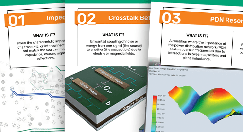
Discover the top 10 signal and power integrity issues causing PCB design failures. Learn how to identify and troubleshoot them for reliable, high-performance circuits.
Read Flipbook
Discover key performance factors that guide PCB material choices, including signal integrity, heat resistance, and durability.
Read Article
Explore PCB design strategies for high pin-count devices with plated through-hole tech. Learn fan-out, routing tips, and power domain optimization for efficient, reliable designs.
Read Article
Learn how constraint driven design in OrCAD X integrates a multidisciplinary approach into the PCB design process to improve reliability and manufacturability.
Read Article
Learn about microvia reliability through failure causes in PCBs with proper design notes, materials, and simulation tools.
Read Article
Learn how to optimize copper current density in PCB design, including temperature, trace width, and via design. Improve reliability with OrCAD X.
Read Article
Avoid costly failures in high-voltage applications with high voltage PCB design guidelines that cover spacing, insulation, material, and best practices.
Read Article
Watch PCB Tutorials or See What's New With Our Design and Analysis Tools
SubscribeIntroduction to best-in-class functional simulation environment and ecosystem powered by PSpice. PSpice and OrCAD X Capture combine to provide industry-leading schematic entry, native analog...
Access Webinar
Read Article
Read Article
Read Article
In this video we will discuss the four reliability features, Schematic Audit, Electrical Stress Analysis, Meantime Before Failure and Power Topology Analysis
Watch Video
Read Article
Lets improve our circuit manufacturing yield using Monte Carlo Analysis in PSpice!
Read Article
Explore common PCB failure reasons and discover advanced OrCAD X features to help identify and prevent them.
Read Article
Easily show components in 3D with OrCAD X. Also learn about features for configuring mechanical enclosures for optimal design integrity.
Read Article
Discover essential tips and considerations for PCB design in military and aerospace applications, including component selection, current capacity, and performance standards.
Read Article
Loading More...