Why HDI Designs Fail in the Field: Advanced Root Causes Beyond Standard Microvia Cracking
When engineers think about HDI reliability, microvia cracking dominates the conversation. Thermal cycling stress, Coefficient of Thermal Expansion (CTE) mismatch, copper fatigue are well-documented failure modes and are increasingly well-managed through improved materials, process controls, and design rules.
But microvia cracking isn't the only way HDI designs fail in the field. A subset of HDI failures originates from subtler mechanisms that may not appear in standard qualification testing yet emerge months or years into deployment. Understanding these advanced root causes helps designers anticipate and prevent failures that conventional reliability analysis might miss.
Resin Starvation
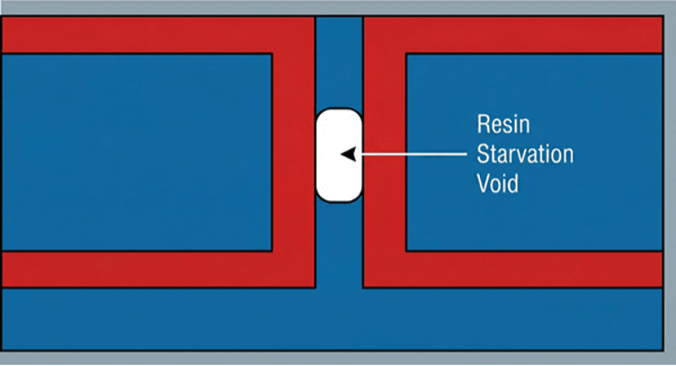
Figure 1. Resin Starvation
During lamination, resin from prepreg layers flows to fill gaps, encapsulate copper features, and bond layers together. Resin starvation occurs when insufficient resin is available to fill all voids, leaving unfilled cavities, incomplete bonding, or inadequate encapsulation of buried features.
HDI designs are particularly susceptible to resin starvation for several reasons. Sequential lamination cycles deplete resin availability: prepreg that has already flowed in an earlier cycle contributes less resin in subsequent cycles. Dense copper features especially filled via pads and thick copper pours displace more resin volume than sparse designs. Fine-pitch geometries create small cavities that are difficult for viscous resin to penetrate.
The consequences of resin starvation range from mild to catastrophic. Minor starvation may cause localized delamination that propagates slowly under thermal stress. Severe starvation can leave voids that trap moisture, creating conditions for conductive anodic filament (CAF) growth or electrochemical migration between adjacent conductors.
Preventing resin starvation requires attention to copper density balancing, appropriate prepreg selection (resin content matched to copper displacement), and lamination process optimization. DFM analysis tools can flag regions at risk for starvation before fabrication, allowing design modifications that improve resin flow.
Copper Pull-Away from Lamination Cycles
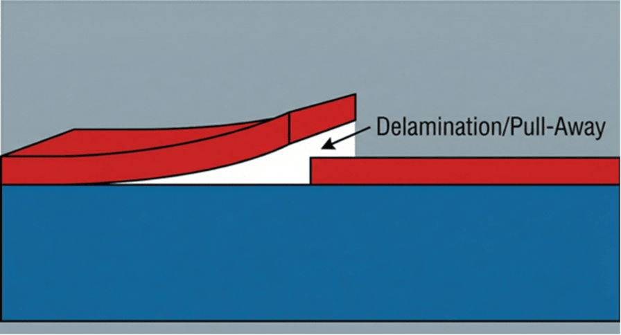
Figure 2. Copper Pull-Away (Delamination)
Each sequential lamination cycle subjects existing copper features to another thermal excursion. Copper and dielectric expand and contract at different rates; adhesion at the copper-dielectric interface must withstand the resulting shear stress.
In conventional single-lamination designs, each interface experiences one lamination cycle plus subsequent thermal events (reflow, operational cycling). In a 3-N-3 HDI design, the innermost core interfaces experience four lamination cycles before the board ever reaches assembly. The cumulative stress can weaken copper-to-dielectric adhesion, particularly at feature edges where stress concentrates.
Copper pull-away often manifests as lifted pads, delaminated traces, or separated annular rings around vias. These defects may not cause immediate failure but create stress concentrations that accelerate crack initiation under operational thermal cycling.
Material selection influences pull-away susceptibility. Some laminate systems maintain adhesion better through multiple thermal cycles than others. Surface treatment of copper (oxide, silane, or other adhesion promoters) also affects bond durability. Designers working on high-layer-count HDI should verify that their material system is qualified for the number of lamination cycles their stackup requires.
Dielectric Collapse Under High Mechanical Stress
HDI stackups often incorporate very thin dielectric layers (only 2 to 4 mils thin) to achieve target impedances with fine traces and to minimize overall board thickness. These thin dielectrics are more susceptible to mechanical deformation under stress than thicker conventional layers.
Dielectric collapse occurs when localized pressure causes the dielectric to thin beyond acceptable limits, potentially allowing copper features on adjacent layers to approach each other or even short. Sources of localized pressure include:
- Component attachment: Press-fit connectors, heat sinks with mounting hardware, and stiffeners all apply mechanical force to the board surface. If this force concentrates over thin dielectric regions, collapse can occur.
- Lamination pressure: Non-uniform pressure during lamination—caused by copper density variations or tooling issues—can make dielectric thinner in localized regions.
- Flexure during handling: Thin boards with thin dielectrics flex more readily than rigid designs. Assembly handling, test fixturing, or operational vibration can create bending stresses that exceed dielectric compression limits.
Design mitigations include avoiding thin dielectrics in regions subject to mechanical stress, using stiffeners to distribute concentrated loads, and specifying handling requirements that limit board flexure during manufacturing and assembly.
Latent Failures That Surface Months After Deployment
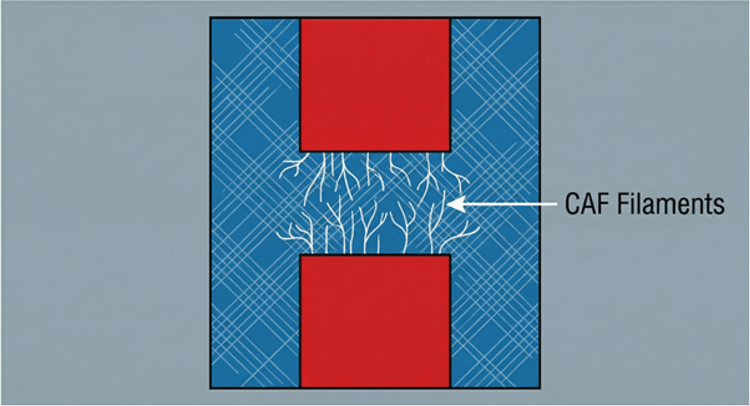
Figure 3. CAF Growth (Conductive Anodic Filament)
Perhaps the most insidious HDI failures are those that pass all qualification testing yet emerge well into field deployment. These latent failures typically result from slowly progressing degradation mechanisms that don't cause immediate failure but eventually exceed the threshold for reliable operation.
Conductive Anodic Filament (CAF) growth: CAF is an electrochemical process that grows conductive copper filaments along glass fiber interfaces in the presence of voltage bias and moisture. HDI designs with tight via-to-via spacing and thin dielectrics reduce the distances these filaments must bridge to create shorts. CAF growth rates depend on humidity exposure, bias voltage, and material susceptibility. The scary part of this problem is that it may take months or years for filaments to span the gap between conductors.
Slow crack propagation: A microvia interface with marginal integrity may survive initial thermal cycling but develop cracks that propagate slowly under operational stress. The via may function correctly for an extended period before cumulative crack growth causes intermittent or permanent failure.
Electrochemical migration: Similar to CAF, electrochemical migration grows metallic dendrites between conductors under bias in the presence of ionic contamination and moisture. Flux residues, fingerprints, or environmental contamination can provide the ionic species needed to initiate migration. Time to failure depends on multiple factors, such as contamination level, humidity exposure, and conductor spacing. These are all factors trending toward aggressive HDI geometries making them more critical.
Solder joint fatigue at HDI interfaces: Via-in-pad designs place solder joints directly over filled microvias. If the via fill isn't perfectly planar, or if the fill material has different thermal expansion than the surrounding copper, the solder joint experiences additional stress beyond what BGA joints on solid copper pads experience. This can accelerate solder fatigue, particularly for high-reliability applications with extended thermal cycling requirements.
Designing for Long-Term Reliability
Preventing these advanced failure modes requires looking beyond standard design rules and qualification protocols:
- Material selection: Choose materials qualified for the specific number of lamination cycles your design requires. Verify CAF resistance ratings match your spacing and operating environment.
- Copper balancing: Ensure copper density is balanced across the board and between layers to promote uniform resin flow and minimize warpage that concentrates stress.
- DFM analysis: Use DFM tools that flag resin starvation risks, annular ring violations, and other HDI-specific concerns before releasing to fabrication.
- Extended qualification: For high-reliability applications, consider extending thermal cycling beyond standard protocols and including humidity exposure to stress latent failure mechanisms.
- Cleanliness specifications: Specify and verify ionic cleanliness levels appropriate for your HDI geometry and operating environment.
HDI technology enables design capabilities that conventional approaches cannot match. Realizing those capabilities without compromising long-term reliability requires understanding the full spectrum of failure mechanisms and designing proactively to prevent them. Especially the not-so-obvious ones.