Reviewing The PCB Design Review Process
One thing for sure about printed circuit board design is that change is inevitable. The vernacular surrounding the art and science of PCB design gives credence to this statement. Up front, it's a schematic editor that leads to a layout editor. If you get far enough downstream, you're working with a Gerber editor. Across the board, the notion of making changes is distilled into the process.
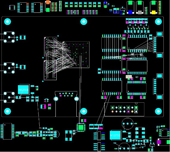
Figure 1. Colorizing power and ground domains helps us floorplan the design. The passive components arrayed across the top of the board are mostly bypass caps destined for the secondary side of the board. The components below are being pre-placed to give more visibility to the extent of these subcircuits. Image Credit: Author.
There's another axiom in effect as well, "If it works, don't break it." This sentiment is especially strong where a circuit must be qualified through a regulatory body. If a radio meets the requirements, it's as if it was written in stone rather than copper. Change is for the better unless it adds unreasonable risk or lengthens the schedule.
It's important to maintain that continuity while making improvements as needed. A second pair of eyes is always helpful and, in fact, the more the merrier up to a point. The mechanical engineering side of a PCB layout is the foundation of the circuit board while the embedded electronics are the vessel for the software. Testing the circuit lies somewhere between these two camps. Herding all of these cats requires a bit of finesse on the part of the PCB Designer.
Getting the Lay of the Land
Kicking off a layout usually starts with the mechanical information. Design reuse of the mechanicals is a common theme. The trick is that later upgrades rarely come in the form of a reduction to the bill of materials. We fix electrical problems with more electronics; perhaps a new filter or a shield. Sometimes, it's another mounting hole and it could be all of those things at once.
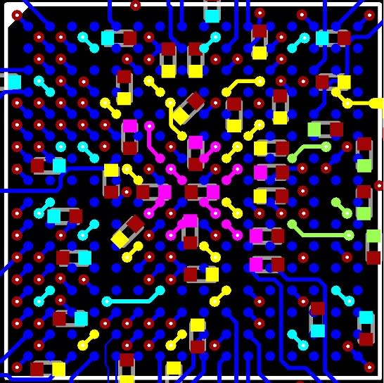
Figure 2. Capacitors on the bottom (red) answer the call for a patch of 1.2V pins (magenta) in the middle of the processor. Surrounding them is a ring of 2.5V in yellow. Finally, the outer voltage domain is for 1.8V (cyan) with a side of 3.3v in green. Completing this PDN is a top priority. Image Credit: Author
We compete in the market with new features to enhance the product. Even with the same feature set, we're compelled towards faster, smaller and more efficient designs. You could say that revision 1 is just messing around while revision 2 is after you find out what was overlooked in the rush to market.
With all of this going on, we can't go it alone. Tight schedules push us into a corner. Back tracking is a waste of that precious time - and money. The goal is always to do it right the first time. All of the above is just to say that we need to have clear communications on every aspect of on-going improvements.
Arbitrary and capricious "changes" can end up back-firing. Don't go at it alone. Schedule a design review at each stage of the design cycle. Day one of the schedule is a good time for setting milestones. Once you have an outline and a stack up you have enough data for a budgetary quote from your vendor(s). "Vendor" should always be plural for the bare board as well as the components.
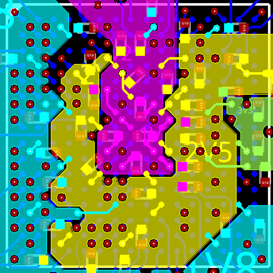
Figure 3. Fan-out optimized for bypass cap placement and avoiding choke points in the power planes. Image Credit: Author
Being Prepared to Kick Off Placement
The mechanical outline and the stackup should account for all of the packages involved as well as the keep-out regions for routing and placement. If you don't want routing below a component type the footprint should include a route keep-out. I build a route-keep-out into every inductor since nobody wants routing under there. There are sensors that require more clearance than a normal part. That extra space should be incorporated into the virtual part.
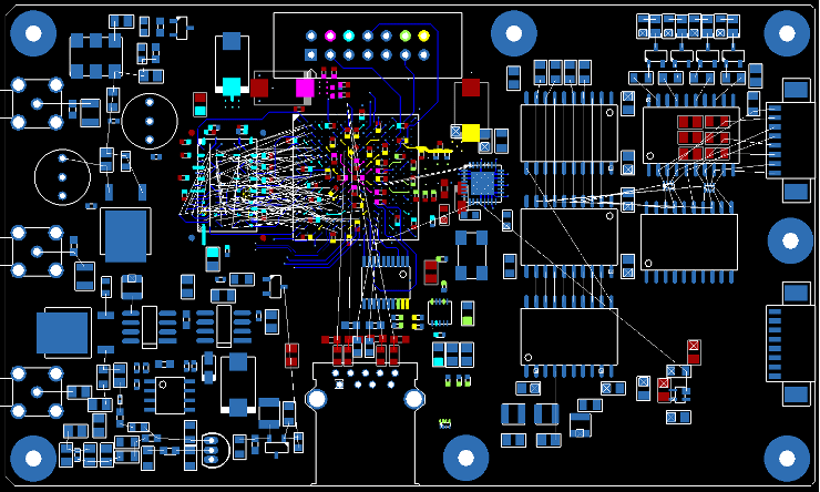
Figure 4. When all was said and done, the board grew in the horizontal while the technology moved from plated through hole to HDI in order to place the DDR memory belly-to-belly. Image Credit: Author.
The more absolute rules you can encapsulate the better. This serves two purposes. One is that it reduces your workload and the other thing is that it shows the reviewers that you're aware of the constraint and have taken action in that regard. Keep-ins, keep-outs, headroom limits and other restrictions can be a hassle but the payoff is a compliant PCBA that fits where it belongs and works as intended.
Design reviews will be boring for someone who has no stake in that part of the process so the attendee list should reflect that. The Mechanical Engineer is required to verify that the board outline and all of the non-electrical features were imported correctly. That's square one. There's no point in inviting the Test Engineer to that review. Loop them in when you've fairly certain that the test points have optimal coverage. By that point, the ME is out of the picture. Their return could be disruptive.
Milestones That Deserve a Design Review
- Mechanical outline review including all components, holes and other features covered by the outline drawing. There may not be an outline drawing at that time. At minimum, we compare the layout to the 3D model to see if everything makes sense. This should involve you and Mechanical Engineering. After this review, it makes sense to spool up the fabricator so they can provide trace geometry and any other input related to the proposed stackup.
- Library completion with all of the components randomly placed outside the board outline. This is you, the EE and maybe CC the Project Manager. If you're lucky enough to have a dedicated Librarian, go ahead and loop them in.
- Critical placement with RF chains routed and major ICs in their proposed locations. You, the EE and Signal Integrity and at least one of your peers if possible.
- Detailed but rough placement with your best effort at fleshing out the power delivery network. This is a good time to organize your reference designators for the first time. Doing so will make the final push a little more bearable. You, the EE, and Power Integrity.
- After fanout is done to the most complex integrated circuits. You and the EE and again, CC the Project Manager. The assembly team, whether in-house or contracted, should be included for a placement evaluation. They can advise you on the Assembly Subpanel and any test coupons as required. Markup every document shared as PRELIMINARY!
- When memory and/or other high-speed signals have been connected and length-matched as required. Bring back Signal Integrity and call on Test Engineering. The EE should be in the loop on a daily basis at this point anyway.
- Routing of the miscellaneous unnamed traces. You, the EE, your Manager and a friend to balance out the power dynamic. After this, your main objective is punching in gratuitous vias for thermal and signal integrity compliance.
- Full documentation package with all design rule errors squared away. Make a print of every layer and each drawing so there's something to mark up. Invite Mechanical Engineering, Electrical Engineering, Project Management, your Manager and the SI/PI team. CC everyone else who made any contribution to the design effort.
Depending on the complexity and nature of a design, some of these may be combined but it still pays to break the job down into milestones so you can tell if the project is on track to meet the tape-out day. Waiting until tape-out day to say that the board isn't done could be seen as a failure on your part; particularly if you've been on "radio silence". Keeping on top of the schedule is a part of managing expectations.
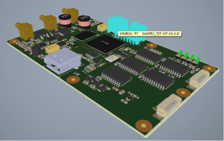
Figure 5. A sanity check after moving the JTAG connector. I will also revisit the inductor between the SMB connectors in the upper corner. Image Credit: Author
The number of touchpoints will vary with each design. Some folks will need a special reminder to make it to the meeting. I remember a signal integrity guy hiding from everyone while using the design review to catch up on his emails. It cuts both ways. Modern times have spread out the workforce so there are likely to be people phoning it in. Make sure that they get a chance to speak and that nobody in the room talks over them.
Schedule the Design Reviews as Soon as Practical
Everyone's calendar fills up by the time they get to work that day. Scheduling these reviews at the start of the layout means that you'll have more flexibility to include the people you need when you need them. This can be done while the schematic is in progress with the schematic-complete milestone penciled in somewhere along the way. Let's be honest here. The schematic will not be done on the day you start the layout.
When things outside of your control happen, it's the only time you can be forgiven for proposing a whole new set of dates for the follow on milestones. Product Managers are under pressure too. They do not want you to pad the schedule for unforeseen circumstances. We act like everything will fall into place at the right moment but it doesn't happen very often.
Hope For the Best While Preparing For the Inevitable
While Sun Tzu often gets credit for it, Helmuth von Moltke said, "No plan survives contact with the enemy." To be clear, your coworkers are not the enemy but they do tend to disrupt the best laid plans. As we work with those around us, we learn who is most likely to come out of the shadows with a last-minute request.
We manage those people the same way we manage an overwhelming concentration of 'rats' coming out of an SOC. Ping them early and often. Ask how confident they are in the input provided at any stage. Some people will hold back on giving you new information until they are certain that it is the best way forward. They keep their cards close to the vest until compelled to share. At the same time, the vendor can't answer questions that were not asked at some point.
I remember at Qualcomm when we onboarded an engineer on a work visa. She was from Australia and informed us that she received the very last visa that was issued for that year. I remarked that she was going to fit right in and added that "If it wasn't for the last minute, nothing would get done around here. It isn't just Qualcomm. It's human nature. It's incumbent upon us to herd those cats as part of getting the job done by the 11th hour when it all comes together.