My OrCAD Journey: 1995-2025+
Printed circuit board design has a long history of innovation. The technology is constantly shifting to new levels of integration. The primary driver for this progress is from the companies that create the components we use. They keep making them smaller for better efficiency and performance.
As board designers, we respond by taking on some of the work previously done at the package/substrate level. The passive components shrink down while the active devices increase their pin density in terms of spacing and overall pin-count. From a schematic point of view, assigning a new and improved footprint for a passive component is straightforward.
The integrated circuits, on the other hand, are broken out into so-called heterogenous-symbols. Unlike memory circuits that tend to replicate, the main logic device has a number of unique circuits. Functional blocks of the circuit are gathered together in a large rectangle that has a fringe of pins around the outside. Input pins are placed on the left side while outputs go to the right. The top and bottom of the rectangle gets populated with power and ground pins, respectively.
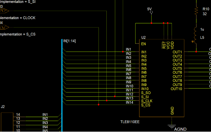
Figure 1. Printed Circuit Boards are the product. The process starts with the schematic as one ingredient among many. Image Credit: Author.
The pins do not bear any relationship to the device as they follow the logic rather than the geometry of the device footprint. When it comes to the BGA style of components, the perimeter of a rectangle doesn't lend itself to matching the physical representation. We would save that effort for the analog block where low pin-counts will be more common. Even then, some baseband devices are packaged in BGA footprints and will require a heterogenous schematic symbol.
This is quite abstract as the many disparate rectangles feature entirely different circuits. The pins are evenly spaced on a grid to ensure that the connections are not misconnected by the width of a pixel. The largest rectangle might have 200 pins but often fewer as the typical bus isn't that wide.
Figure 2. The time honored method of schematic symbol definition is something that reads left to right for signals and top to bottom for power and ground. This is recommended for digital circuits. The nature of analog circuits calls for a schematic symbol that reflects the actual PCB footprint in terms of pin orientation. This is true of filters, diplexers, dividers, circulators and other low pin-count RF devices. The notion is to use concrete symbols where you can and abstract ones when you must. Image Credit: Author
When it comes to integrated circuits, "we've come a long way, baby". My first edge-router, circa 1999, featured four processor cores that were packaged in 476 pin BGA packages. There was a fifth large chip used as a memory controller. That adds up to around 2300 pins for the CPU. Add more pins for the solder-down memory and the obligatory socketed memory for future expansion.
Today's version would have way more than four processor cores but all of them would be on the same piece of silicon which would also include the memory controller. The modern device has maybe 1200 to 1400 pins but would be a fraction of the size of the 476 pin BGA of yore.
That old schematic had 29 D-size pages that were jam-packed with circuitry. The D-size paper is about as wide as you can stretch your arms. In those days, we would actually blueprint the schematic at full size. We would have a highlighter and a mark-up pen to use as we went through initial placement.
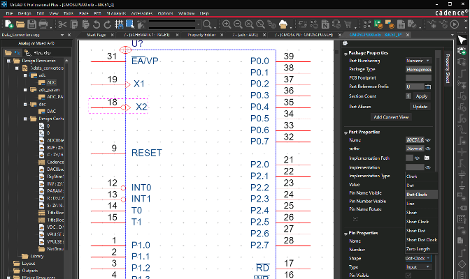
Figure 3. The symbol editor allows for several pin types including the dot for an inverted pin (pins 12 & 13) as well as clock pins (19) and an inverted clock pin (18). The three bus lanes, (P0, P1 and P2) are bidirectional I/O pins. It would be the designer's option in terms of which side to use so this symbol uses both sides for a more balanced pin density. One thing to remember: The pin numbers for miscellaneous ground pins should follow a consistent naming convention in alignment with the PCB footprint library. Image Credit: Author
One of the main things to mark up is when there were multiple logic gates in a package where you could use whichever one you wanted. During placement, it would become obvious that we needed to rewire the circuit for cleaner routing.
Let's say you have a hex inverter in front of a quad XOR-gate. We could clean up ugly routing between those chips by doing logical gate-swaps. This would allow us to comb out the tangled traces into a perfectly organized flow. At that point, we could create a netlist within our ECAD tool and back-annotate that to the schematic. This might seem like the tail wagging the dog but it was a powerful process that was supported by OrCAD regardless of which ECAD software was in use.
Back then, OrCAD didn't have a layout option, it was a tool-agnostic schematic capture platform that could export a large number of different netlist formats. Even before the edge-routier design, I got to use it to capture a two-page schematic that existed in a different schematic software. One of our potential customers, AT&T, asked the company to generate an OrCAD schematic for their internal consumption.
That task was passed down to me. It took some time since I had to learn how to generate the symbols that were not already in the library while learning to use OrCAD "by the seat of my pants." I kept my head down and got it done. The late-80s version of OrCAD had a really nice feature that automatically created a block diagram for each page of the schematic using the off-page net labels within each page.
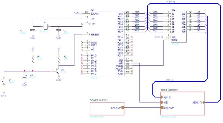
Figure 4. It looks like I accidentally moved pin 18 when I was messing around with the pin types since it is no longer connected to Y1. Meanwhile, the red boxes at the bottom of the image represent a collection of symbols and connections. Hierarchical schematic symbols like this allow for independent parties to collaborate in real time. Image Credit: Author
That diagram was the page that loaded when starting OrCAD. To go to a specific page, all you had to do was click on the desired block. Make some edits to a net name and the next time you went to the block diagram, everything was updated. That association meant that the block diagram was as accurate as the underlying data. By the time I finished those two pages, I was smitten. Our old schematic capture tool was no longer as alluring.
One of the issues with the old tool was that it was difficult to archive a design with any expectation that you could reconstitute it later. Every symbol was written out as a .txt file that had to be saved along with the schematic file. Any missing or inaccurate .txt files would manifest as a white rectangle surrounded by dangling wires where the symbol should have been.
That perceived flaw didn't sit well with my manager. He came to me and gave me a new task. I was told to learn the ins and outs of every schematic capture tool on the market and to write a report that recommended the best way forward. I knew from the tenor of the assignment that our current software was not going to be the winner.
So I went to factory training on Veribest (now Siemens) and Protel (now Altium) then self-taught on several other schematic capture packages. In the end, it was OrCAD that took the prize although Protel had the prettiest interface and Veribest had unmatched integration within its ecosystem.
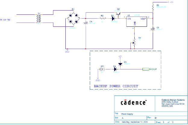
Figure 5. Double clicking the power supply box takes us deeper into the hierarchical schematic. In this way, different subject matter experts can own different parts of the schematic. We do have to be aware of multi-gate packages to ensure that they end up with the same reference designators. Otherwise, the netlist will have two or more PCB footprints where it should all be in one package.
You probably know that Cadence is one of the market leaders in the eda space and as a rule, I'm not going to have anything negative to say about the competition. My goal is to shine a light on OrCAD without casting shade elsewhere.
The library symbols that I captured for AT&T made up about 80% of the typical new job which improved over time. That part of the changeover was not as hard as I anticipated. As luck would have it, OrCAD was acquired by Cadence not too long after the edge-router design was complete. It has become more integrated with Allegro and has spawned a light version of it under the OrCAD banner.
Switching between the two isn't very hard but my fingers know how to use hot keys based on Allegro first and foremost. An example of this would be the command to edit text. Allegro uses alt-E-T, while in OrCAD layout, it's alt-E-X. The menus are slightly different but the sub-menus where the work goes on are pretty much the same across the board. While I prefer Allegro, OrCAD is not much of a step down. If I was spending my own money, it's the OrCAD suite all day long.