Pre-Tapeout Confidence: In-Design Checks for Power Integrity in Allegro X
The layout looks done. Components are placed. Traces are routed. The 3D view shows a nice, compact board that fits the USB-C adapter enclosure.
Time to send it out for fabrication?
Not yet.
What you're looking at is a design that might work. You've followed best practices. You've kept the hot loop tight. You've maintained isolation spacing. But until you run the checks, you don't actually know.
Pre-tapeout verification is the difference between confidence and hope. For a 5V/2A USB-C adapter, where margins are tight and failures are expensive, hope isn't a strategy.
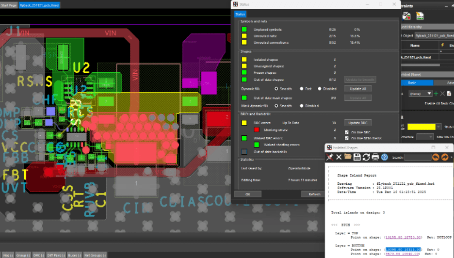
Verification analysis from design rule check (DRC)
What "Power Integrity" Actually Means
Power integrity is a simple question with complicated answers: Does the power delivery network do its job?
For your 5V output, that means:
- Voltage at the load stays within tolerance under all conditions
- Transient response is fast enough when load steps up or down
- Noise and ripple stay below limits
- Thermal performance keeps copper and components within ratings
These are key performance indicators for any board and require analysis.
Before running IR-drop, return-path, and spacing verification checks, it helps to understand how current flows through a power delivery network and why return paths, loop inductance, and grounding directly impact power integrity. This on-demand webinar on the physics-based foundations of power supply design provides useful background for interpreting these analyses.
The Three Checks That Matter
Check 1: DC IR-Drop
What it answers: How much voltage am I losing between the power source and the load?
Every piece of copper has resistance. Current through resistance drops voltage. For a 5V/2A design, losing 200mV to trace resistance means your load sees 4.8V-potentially outside spec.
How to run it:
In Sigrity X (integrated with Allegro X), you define current source points and sink points. The tool calculates voltage at every point based on actual copper geometry.
For this design:
- Source: Output capacitor positive terminal, 2A
- Sink: USB-C connector power pins, 2A
- Include the return path through ground
What to look for:
- Total drop: Should be a small fraction of output voltage. For 5V, I target <100mV (<2%).
- Hot spots: Where is the drop concentrated? Usually in narrow traces, via transitions, or plane necking.
- Asymmetric drops: If the power trace drops 30mV but the ground return drops 100mV, your ground path is the bottleneck.
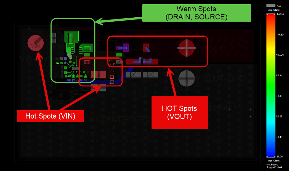
IR-drop color map of the input and output power paths. Warmer colors show higher drop.
Check 2: Return Path Continuity
What it answers: Does the return current have a clean path back to its source?
High-frequency currents return directly under the trace that carried them forward-that's the lowest inductance path. If something forces a detour, loop area increases, inductance increases, and EMI increases.
How to run it:
The return path analysis in Sigrity X visualizes current density on the ground plane. You can see exactly where the return current flows.
What to look for:
- Narrow channels: Return current should flow in a concentrated channel under the forward trace. If it's spreading widely, something is forcing it off the ideal path.
- Detours around obstacles: Plane splits, via fields, or keepouts that force return current the long way around.
- Layer transitions: When a trace changes layers through a via, the return current needs a nearby via to follow. Missing return vias force detours.
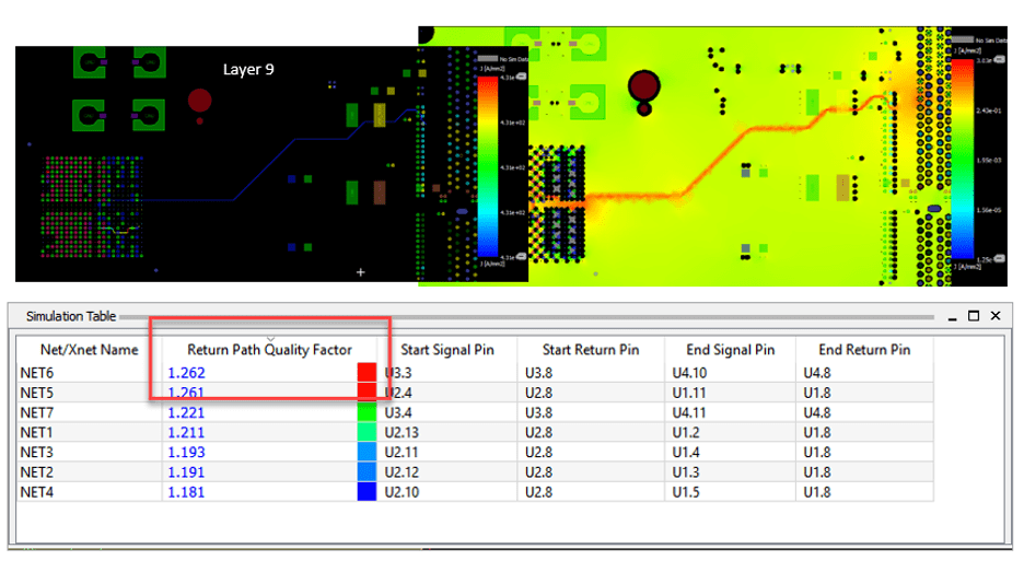
Return path analysis showing current density on ground plane (Cadence).
Check 3: Isolation Spacing DRC
What it answers: Have I maintained required creepage and clearance everywhere?
For an offline flyback, the isolation barrier between primary and secondary is a safety requirement. Even a single violation - such as a via placed too close or a trace that creeps into the boundary - can result in failing safety certification.
How to run it:
With constraints properly configured in Allegro X (primary region, secondary region, spacing rules), you run DRC. Every violation is flagged.
What to look for:
- Zero violations: That's the target. Any violation needs to be fixed before tapeout.
- Near-misses: Look at the smallest actual spacing. If you're at 6.5mm and the requirement is 6.4mm, you have 100µm of margin. Is that enough for manufacturing tolerance?
- All layers: Isolation must be maintained on every layer. A via on layer 3 that's too close to copper on layer 2 is still a violation.
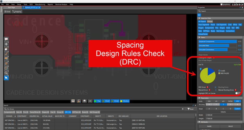
DRC results showing various spacing checks
Running the Checks in Practice
Here's the sequence I follow before releasing a design for fabrication:
Step 1: Final DRC on design rules. Trace width, spacing, via sizes. Clear all violations or document exceptions.
Step 2: IR-drop analysis on power paths. Output power, ground return, and any intermediate rails. Confirm drop is within budget.
Step 3: Return path visualization on switching nets. Hot loop traces, gate drive signals, any high-frequency paths. Confirm no forced detours.
Step 4: Isolation spacing DRC. Run the specific check for primary-to-secondary spacing. Zero violations is the standard.
Step 5: Document results. Export reports and screenshots. These become part of the design package for traceability.
This sequence takes maybe an hour for a 10W adapter design. The cost of skipping this sequence is often weeks of debugging, and possibly board respins, and even failed certifications.
What These Checks Catch
Real examples of issues found during pre-tapeout verification:
Case 1: Ground plane necking. IR-drop analysis showed 150mV drop in the ground return-way more than the 50mV in the power trace. The ground plane narrowed to 15 mils where it passed between two mounting holes. Widening the passage dropped the return path resistance by 60%.
Case 2: Missing return via. Return path analysis showed switching current spreading across the entire plane when crossing from layer 1 to layer 2. A signal via transitioned layers but no ground via was nearby. Adding a ground via stitched the return path and contained the current flow.
Case 3: Via encroachment. Isolation DRC found a via on the secondary side 5.9mm from primary copper-violating the 6.4mm requirement. The via wasn't part of any routed net; it was a thermal via for a secondary-side component. Removing it cleared the violation.
Confidence, Not Hope
Tapeout should feel very confident, but oftentimes it feels like you're crossing fingers, hoping it will go right.
How do you feel more confident in the tapeout? That confidence comes from verification. You've run the analysis. You've seen the numbers. You know the IR-drop is within budget, the return paths are clean, the isolation spacing is verified. The design works-and not because you think it should, but because you've measured it.
Hope is sending the design out with crossed fingers. Maybe the ground path is fine. Maybe the isolation is adequate. Maybe it'll pass testing on the first try.
For a 10W USB-C adapter, the stakes are real. A board respin costs more money and time than engineers and management are willing to admit. A failed EMI test delays the product launch. A failed safety certification stops the product entirely. And engineers scrambling, working 10 to 12-hour days to fix the problems.
Pre-tapeout verification is basically cheap insurance at this point.
The Takeaway
Before you release the design, run the following checks:
- IR-drop analysis - Voltage at the load, not just at the capacitors
- Return path continuity - Current flows where you expect, without detours
- Isolation spacing DRC - Verify every primary-to-secondary gap in the design
Document the results. Include them in the design package. When someone asks "how do you know it works?"-show them the analysis. That's also a good way to impress your managers.
That's real pre-tapeout confidence.