Thermal & EMI in Power Supply Design: The Physics Your Schematic Won't Show You
"Why does my power supply pass the design review but fail in the EMC chamber-or start thermal throttling three months after it's deployed?"
Key Takeaways:
- EMI and thermal problems are architecture decisions, not layout afterthoughts
- Current loops determine your EMI fate-not the schematic, not the BOM
- Spreading heat early beats adding heatsinks later
- Simulation catches 80% of problems before the first board spin
The Board That Worked (Until It Didn't)
A colleague shipped a power supply that passed every bench test. Clean waveforms. Tight regulation. Efficiency numbers that made the datasheet look conservative.
Six weeks later, field returns started coming in. Units shutting down randomly. No pattern anyone could find.
The root cause? A MOSFET running 15°C hotter than predicted. Not because the calculations were wrong-they were textbook perfect. Because the enclosure airflow in the customer's rack was nothing like the open-bench conditions where the design was validated.
The schematic was correct. The simulation was correct. The architecture-where hot components sat relative to airflow, how losses were distributed across the power tree-that's where the problem lived.
Here's the uncomfortable truth: thermal and EMI problems don't show up in your schematic. They hide in your architecture decisions. And by the time you discover them, changing architecture means re-spinning the board.
If you want to understand the physical mechanisms behind thermal and EMI interactions in power supply design, this on-demand webinar on the physics-based foundations of power supply design explains how energy dissipation, current paths, and field effects combine in real systems beyond schematic-level assumptions.
Why Bench Tests Lie
On your bench, with a DMM and a modest load, almost anything "works."
The real test comes when:
- The enclosure is sealed
- Ambient temperature is 45°C instead of 25°C
- Multiple rails are switching simultaneously
- Cables turn your neat design into an antenna farm
Suddenly, junction temperatures spike. The EMC lab sends you a report decorated with red bars. And your project manager wants to know why the schedule just slipped three weeks.
The gap between "works on bench" and "works in production" is exactly the gap this article addresses.
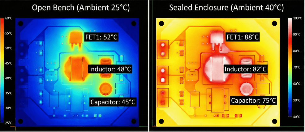
Thermal camera comparison: The 30°C difference between bench and deployment
Thermal: It's Architecture, Not Heatsinks
When I hear "we'll fix the thermal issues later," I know that project is about to get expensive.
Here's where your power supply's heat actually comes from:
- Conduction losses - I²R in MOSFETs, diodes, inductors, copper traces
- Switching losses - voltage/current overlap during transitions, gate drive energy
- Magnetics losses - core losses plus copper losses in windings
- Controller overhead - gate drivers, PWM controllers, housekeeping rails
Your architecture determines where those losses concentrate. Multi-phase bucks spread current across multiple devices. Synchronous rectification shifts loss from diodes to MOSFETs (where it's easier to heatsink). Topology choice drives peak and RMS current profiles.
The trap: you keep stacking features-higher frequency for smaller magnetics, tighter layout for shorter traces-until you've created a thermal density your mechanical team simply cannot fix.
I've seen engineers argue with mechanical designers about heatsink height when the real problem was choosing a topology that concentrated 8W of loss in a 5mm × 6mm QFN package. No heatsink geometry in the world solves that problem elegantly.
EMI: Fields Follow Current, Not Schematics
EMI doesn't care about your netlist. It cares about physics.
Radiated emissions are driven by three key factors. High di/dt current loops, such as those in switch node, rectifier return path, and gate drive circuits. High dv/dt nodes, like switching nodes capacitively coupling into nearby components. And cables acting as antennas, like that 18-inch wire you overlooked, which becomes a perfect broadband radiator.
Your architecture choices set the stage for EMI long before a single trace is routed. These include decisions like where to place the power stage relative to sensitive analog or RF sections, and whether isolation is needed since transformers create common-mode noise paths. Additionally, switching frequency selection determines where harmonics land relative to regulatory limits, and the ground partitioning strategy, whether it's star, plane or split.
A perfectly compensated, beautifully efficient supply can still be an EMC disaster. I've watched designs fail FCC testing because loop area wasn't considered during component placement. The fix required a board re-spin-not a filter tweak.
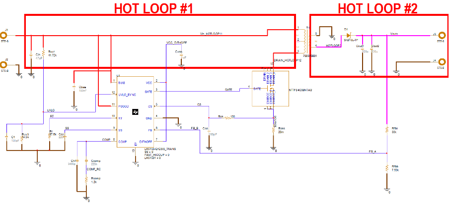
The loop your schematic doesn't show—but the EMC lab definitely finds.
Practical Thermal Guidelines
These aren't textbook rules. They're what actually prevents thermal re-spins:
1. Budget losses per block early
Before you finalize your topology, assign rough loss budgets:
- Primary switch: X watts maximum loss
- Rectification: Y watts maximum loss
- Magnetics: Z watts maximum loss
Quick calculations plus early simulation tells you if the numbers are even feasible before you're committed to the rest of the design.
2. Spread heat where you can
- Multi-phase converters for high-current rails
- Hot devices against copper pours with thermal paths to chassis
- Don't cluster all high-loss components in one corner with no airflow path (they get really hot and even some air flow helps a lot)
3. Design for worst-case scenarios, not typical cases
Design for maximum ambient temperature. Account for aging derating. Account for the design operating at full load. Take all these factors into account simultaneously. That's your design point. Not the 25°C bench with only 50% load. In fact, stress test the load (e.g. test 2.5 Amps or 3 Amps on the load for a design meant for 2 Amps).
4. Talk to mechanical before layout
Mechanical limits come before PCB layout. Even before electrical engineering. So, share power loss maps, not just electrical schematics. Let thermal engineers influence component placement while you still have the freedom to route traces. Because if you wait until after layout, your options are limited to "add a bigger heatsink" and "add a fan" - neither of which is elegant and may not solve the core problem. Not only do we need to consider PCB layout, let's look at electromagnetic interference (EMI).
Practical EMI Guidelines
Many engineers wait until PCB layout to do EMI analysis and simulation. But EMI compliance starts at the system hardware block diagram, not the layout review. Let's address ways to do good EMC design:
1. Zone your board
On your block diagram, mark:
- Noisy blocks (switching power stages)
- Sensitive blocks (analog front ends, RF, precision references)
Plan your PCB stackup and floorplan to keep them separated. This is an architecture decision, not a layout detail.
2. Think in loops, not nets
Every high-frequency current has a return path for the EM field. That return path plus the outgoing path forms a loop. Loop area is your antenna. Minimize it at the architecture level-plan for solid return planes under power stages from the start.
3. Plan your isolation strategy
For isolated supplies, decide early:
- Where does the secondary side of your transformer reference to the primary side return path (if at all)?
- Where do Y-capacitors (for EMI filtering and ground bridging) go?
- How do cable shields connect to chassis?
4. Frequency planning isn't optional
Don't pick switching frequencies randomly. Consider:
- Where harmonics land relative to FCC/CE limits
- What other switching supplies and clocks exist in your system
- For multi-rail designs, stagger phases or frequencies to avoid additive peaks in the EMI spectrum
When Your Organization Scales
Here's where mid-sized companies get bitten.
You move from one main product to a portfolio. Different teams reuse power supply blocks across multiple products (SKUs). Enclosures change. The environment airflow changes. Even the cable lengths change.
Compliance issues on one product start surfacing in others. The senior engineer who knew why certain layout choices were made has moved to another project. Knowledge walks out of the room.
What you need is a reusable architecture playbook:
- Standardized stackups and placement rules for power stages
- Known-good EMI filter patterns and layout templates (great for design reuse and place-replicate-create options)
- Thermal "do not exceed" maps for reference designs
This lets engineering managers approve new designs quickly. It lets junior engineers avoid classic thermal and EMI landmines without needing twenty years of scar tissue.
Where Modern Tools Actually Help
The old workflow: design the schematic, lay out the board, spin it, test it, discover thermal or EMI problems, re-spin. Repeat until the schedule collapses or the budget runs out.
The new workflow involves assessing these conditions beforehand.
In an Allegro X environment, you can address these concerns far sooner:
Use PSpice early for loss estimation:
- RMS and peak currents in MOSFETs, diodes, inductors
- Switching waveforms that predict EMI behavior
- Duty cycles across worst-case scenarios-not just typical operation
Use Allegro X with Sigrity for power integrity:
- Visualize current return paths and identify large loop areas
- IR drop analysis to find where heating concentrates
- Evaluate plane splits and stitching vias that affect both EMI and thermal distribution
Capture best practices as constraints:
- Keep noisy loops and sensitive traces separated by rule, not by memory
- Reuse proven floorplans instead of reinventing them per project
The goal is moving from "fix it in the lab" to "design with compliance baked in." That's what medium-sized organizations need as they scale into enterprise-grade products.
Quick Reference: Thermal & EMI by Architecture Choice
|
Architecture Choice |
Thermal Implication |
EMI Implication |
|
Multi-phase buck |
Spreads loss across devices; easier to cool |
Multiple loops to manage; phase staggering helps EMI |
|
Higher frequency |
Switching loss increases; smaller magnetics may run hotter |
Harmonics shift up; watch regulatory bands |
|
Sync rectification |
Shifts diode loss to FET; can heatsink FET easier |
Adds high di/dt loop; gate drive returns matter |
|
Isolated flyback |
Transformer losses add up; clamp/snubber dissipates too |
Common-mode noise across isolation barrier |
|
Compact layout |
Higher thermal density; hotspots concentrate |
Smaller loops possible; but coupling increases |
The Real Lesson
Thermal and EMI aren't problems you solve at the end. They're constraints you design around from the beginning.
The engineer who thinks about current loops at the block diagram stage spends less time in the EMC lab. The engineer who budgets losses before selecting components doesn't argue about heatsink height later.
Your schematic captures the electrical intent. Your architecture-topology choice, placement strategy, grounding philosophy, thermal distribution-determines whether that intent survives contact with physics.
Design for the enclosure, not the bench. Design for worst-case, not typical. And simulate before you spin another set of PCBs.
That's how power supplies get designed in industry. Not by heroic debugging after the fact. By architecture that anticipates the problems.
Now you know the approach. You can use this any time.