Tips on Creating a PCB Footprint For Printed Circuit Board Assemblies
We all start somewhere. My first attempts at PCB layout were single-layer RF amplifiers and were created from a hand-drawn schematic without a net list. The parts were built from the catalogs that PCB Designers collected from their favorite component vendors. We used AutoCAD and created sub-blocks for the part footprints. The traces were more like free-form shapes.
At that time, the boards were fabricated and assembled in-house. We didn’t have the means to apply a solder mask or silkscreen. A thin-layer GTEK material was bonded to aluminum “pallets” for stiffness and thermal conductivity. If one trace had to cross another, the less important one had a series resistor added to allow the other trace to pass below.
We were one step up from designing these boards by hand in the 1990s. We put rubylith into a pen plotter and replaced the pen with a metal point to cut the circuit pattern from the CAD data. Then we had to peel away the areas that were to become air gaps. Our machinist would complete the circuit pattern with that mylar as a phototool and then bond the PCB material to the aluminum pallet. The assemblers took it from there.
PCB Footprints For Today’s Products
“Our goal is to reduce the length of the list of exceptions that the fab shop gives us as a reply to our request for a quote.”
Times change. Your factory is more likely to be in another country than in another room of the same building, particularly for consumer hardware. We’re not pushing a design over the wall; it’s crossing an ocean to people who are already a day ahead of us. The manufacturing flow compels us to get ahead of the details that crop up in the DFM cycle. Our goal is to reduce the length of the list of exceptions that the fab shop gives us as a reply to our request for a quote.
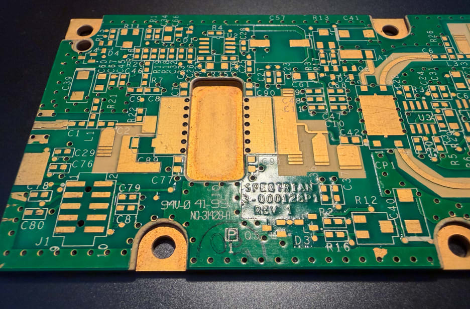
Figure 1. Cellular basestation amplifier circa 1999. Analog components may require specific machining in addition to their land pattern. Meanwhile, the routing around the socket involves numerous tuning stubs sprouting from the traces. Note that this is a 4-layer board with heavy copper as the base. Image Credit: Author
The first thing we consider when creating footprint geometry is what level of reliability is required. By default, we adhere to IPC-6012 Class 2, which covers enterprise electronics excluding aerospace, defence, and medical electronics, where Class 3 prevails. If we put Class 2 in our fabrication notes, then we should put Class 2 into our PCB footprints. That’s what I’m going to use as a basis.
Plated Through Hole Components
Square one is the padstack. The through-hole parts will have their drill size, which determines the size of the capture pad for each layer. Outer layers tend to require a slightly larger pad than inner layers. The expansion of the capture pad is based on the upper tolerance for the hole size. We’re also factoring in the allowance for misregistration from layer to layer.
That’s pretty easy with a one-layer board, but it gets more involved as the layers stack up. Vias would typically take the high end of the finished hole size range and add 50 micrometers (two mils) on the inner layers and a little more on the outer layers. Solderable pads would have to increase by at least 127 microns (five mils) on those outer layers in order to create room for a solder fillet. Bigger is better if there is no impedance penalty. More metal to anchor the pad is good for fabrication and longevity.
Surface Mount Components
Surface mount (SMD) devices get more done with less space. As the name implies, they attach to one side without protruding into the inner-layer routing channels or the mounting surface on the other side of the board. This is the technology to use in a competitive environment. Combining SMD components with High Density Interconnect (HDI) construction opens the door to more advanced microelectronics. We can populate both sides of the board more or less independently.
As the components and printed circuit boards shrink, we lose the traditional space to include component outlines, reference designators, and even the polarity marking. They drop out in that order. We may have to give up fiducial marks and any board-level marking. The keepers are on the positive lead of diodes, polarized capacitors, and integrated circuits.
Increased Placement Density Considerations
At some point, the IPC Class 2 rules get in the way. The reproducibility of Class 2 is surrendered. One of those nice-to-have features is the solder dam between pads. Our options would be down to gang-relief or using lasers to sculpt the solder mask openings. That second option is expensive and harder to find. We have to consider that as we build our library.
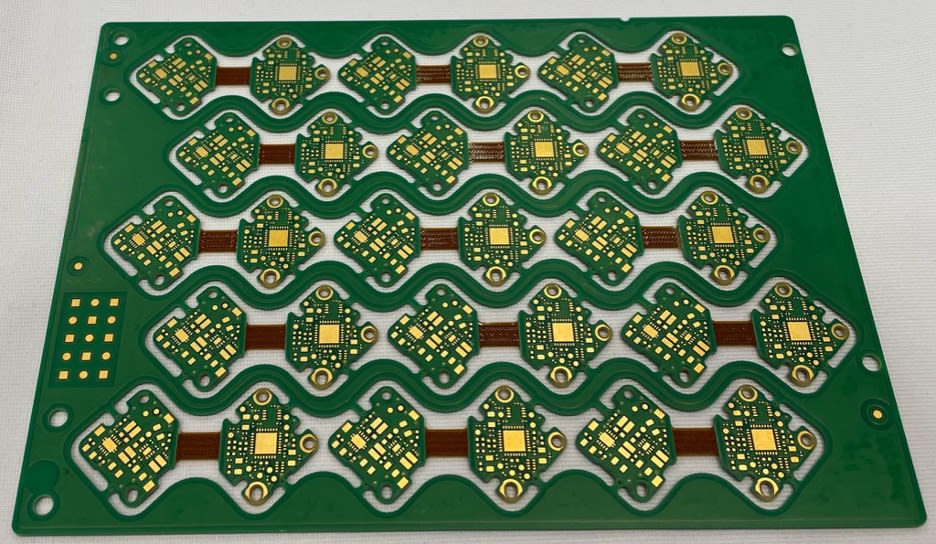
Figure 2. A leading edge rigid-flex circuit with no marking as an example where the form-factor drives the component generation. Image Credit: Author
Knowing that one size does not fit all, IPC breaks this out with a three-tiered approach using A, B, and C to designate Good, Better, and Best. These three categories track along with Class 1, 2 and 3 fabrication levels, but we’re not required to “stay in our lane” unless there’s something contractual involved.
Lines and Letters On The Printed Circuit Board
Creating a PCB footprint will usually include linework that depicts the assembly, along with another one that clears away from the pads and mask openings for the silkscreen. The silkscreen line will be more realistic if it is drawn with a 150 micron (six mil) stroke.
The line should be clear of the pad and soldermask by an additional 76 microns (three mil) to allow for misregistration of the mask and ink layers. If you don’t expand the soldermask layer around the pads and widen the silkscreen lines, it is very easy to get silkscreen on the pads. Of course, you can use a fabrication note to tell the vendor to make sure no ink gets onto the exposed metal. Life is going to be easier for everyone if there is no stray ink to begin with.
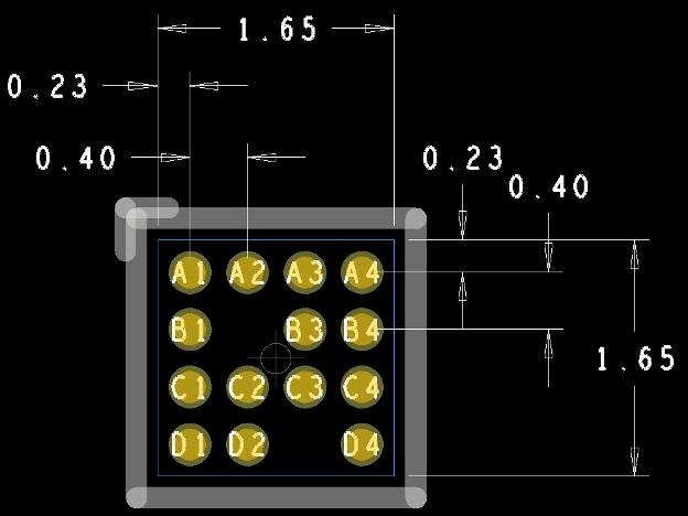
Figure 3. A DFM-sensitive digital twin will include dimensions in a manner that echoes the data sheet for easy checking. Silkscreen and soldermask expansion meet the goals for the class. The origin of the part facilitates pick and place automation while the pin numbers fit within the pads for legibility. Image Credit: Author
When you apply this concept to a part smaller than an 0603 size component, the silkscreen starts to overlap when you place the passive components in tight proximity. It’s better to omit the silkscreen for the outline for the 0402 and below classes of components.
When it comes to high pin-count connectors, a tick mark for every 10th pin would be a nice gesture. The pins are small. They’re close together, and then you have to find pin 47. A connector with a large component keep-out around it is prime for this kind of extra information.
In Conclusion
There are so many considerations when it comes to creating a library of components that are fit to use. The usual conflict is when the component vendor is out in front of the fabricator in terms of achieving precise tolerances. A solid library process will get ahead of these issues with awareness of their vendors’ capabilities. The limits of the fabrication and the assembly vendors are not a secret. A good landing requires a good library right from the launch.