Splitting a Printed Circuit Board For Concurrent Design
Printed circuit board design grows in complexity with each passing year. There are many protocols to implement. An ASIC or an FPGA may be the center of attention but there will likely be a memory bus along with other architecture such as Ethernet or USB to move data around. Interacting with the world around us will require some sort of sensor to read the room while other circuits are used to feed this processed data back to the user.
As mixed signal designs become more common, it makes sense to divvy up the work to those who have the necessary skills. Printed circuit board designers tend to fall into a specialty. Their first job becomes an anchor that pulls them back to that same technology.
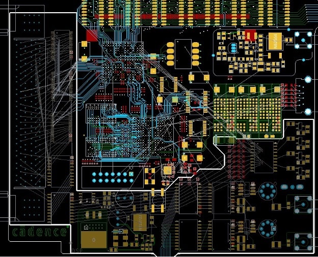
Figure 1. The initial partition is gerrymandered from the upper left to the lower right containing 108 components. Note that the components within the partition are dimmed and locked from editing. There is a small pocket in the upper right corner with 38 components that might be worth another partition. Image Credit: Author
At least, that’s how it worked for me and analog layout. I didn’t see a DDR memory device until 2013. By 2017, the DDR was stacked above the processor, eliminating the whole routing effort. When I got to the XBOX One X main logic board, the DDR5 was a beautiful twelve-package array that was locked down and off limits. While I have struggled through the constraint capture and routing of a smaller DDR3 memory circuit, I’ll never be an expert.
Compartmentalizing the board needs to follow the high level placement as a minimum. This floorplanning revolves around the SI/PI goals. Identifying and capturing the design parameters is a must before anything gets turned loose. As the owner of the deliverables, it’s best to concentrate on the PDN study since it’s everywhere. You can optimize bottlenecks and other conflicts of interest early in the design cycle.
The second priority in defining a partition is to minimize the number of connections in and out of the circuit block. The overall placement is going to drive the flow of data. Routing to an SD card or some other I/O is often suboptimal in terms of trace length. These inevitable rivers of traces can and will be routed from one partition to another. The person working inside the box will see where the traces come in and will be able to go from there.
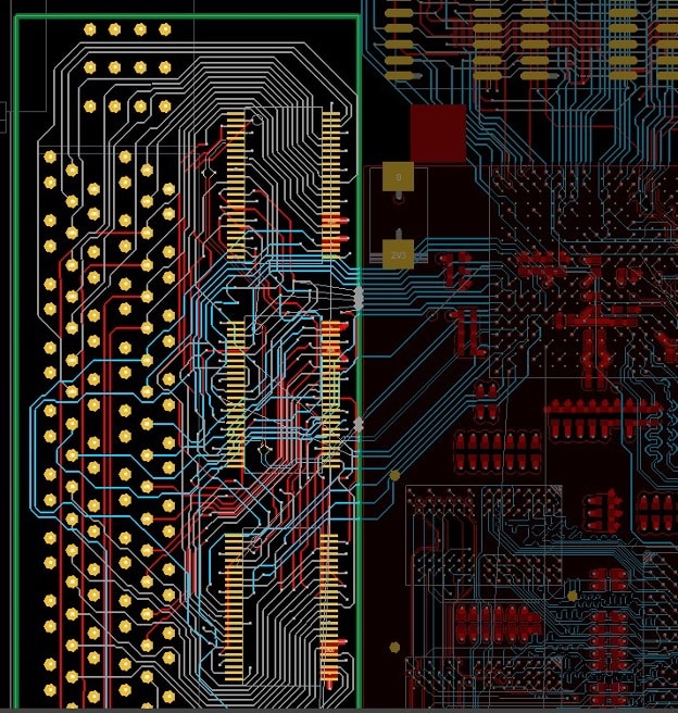
Figure 2. This is the point of view while working inside the partition. Completing the connections that span from the dark side to the bright side is a high priority. We have a few left here that can be completed when the layout is all together. Image Credit: Author
Our use case involved a service bureau and an internal resource with me in the driver’s seat. A hierarchical schematic may not be for everyone but, in this case, it allowed us to decouple from the wireless portion of the design. That’s a high-touch effort so we kept it in-house. For reference, this was a break-out board for a smart phone. The main function was to measure current plus the typical P1 “experiments” that you do when it’s two years before production starts.
The RF section was essentially “Set it and forget it.” It’s like when you’re playing volleyball and one of your teammates is 6’5” (2 Meters) tall. They got this. My day-to-day was under the footprint of the Qualcomm chip. At that point in time, the chip didn’t exist and neither did a reference design. I got to fan out my very own Snapdragon!
The Power Integrity lady sent me back to the drawing board three times before signing off. It came with a warning not to change any of the shapes, not even a little. It was then that I understood the people at Qualcomm telling me not to touch the SOC while routing the SDIO lines out back in the day. Mobile chips are very sensitive to power distribution. Solving all of this drama makes me want to stick with radio boards.
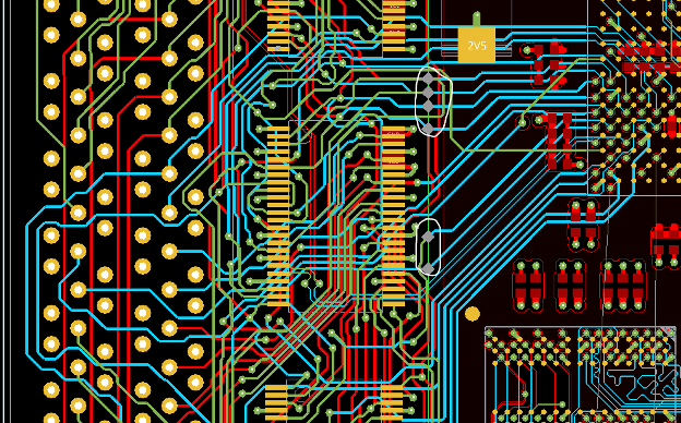
Figure 3 The side job and the main job have been merged. Result: the big connector is squared away. Lesson learned is that I put more space between the guideposts (grey diamonds) that pre-set the cross-over points. With the left edge secured, we will have new instructions and primary routing to the southern edge done before exporting the partition again. Image Credit: Author
Meanwhile, the service bureau had a large board area sectioned off with some big connectors on one end and a whole bunch of op amps and sense resistors to enable across the board. I fanned out one big connector to the LC filters and told them to do the others the same way. Leaving them a few examples was better than hoping that they read my mind.
At some point, all of the things had to be brought back together under one design. Importing the completed section could end up taking a few hours. I learned some things about documenting what’s inside the partition before sharing. It’s very easy to make a list of the components in an area.
It would have saved me some time to set up the display and other options with a script. Playing back the script would have reset the environment to the exact conditions so that everything comes back as planned. I encourage the satellite workers to start a script that can play back their contribution if the reimport process runs into a jam.
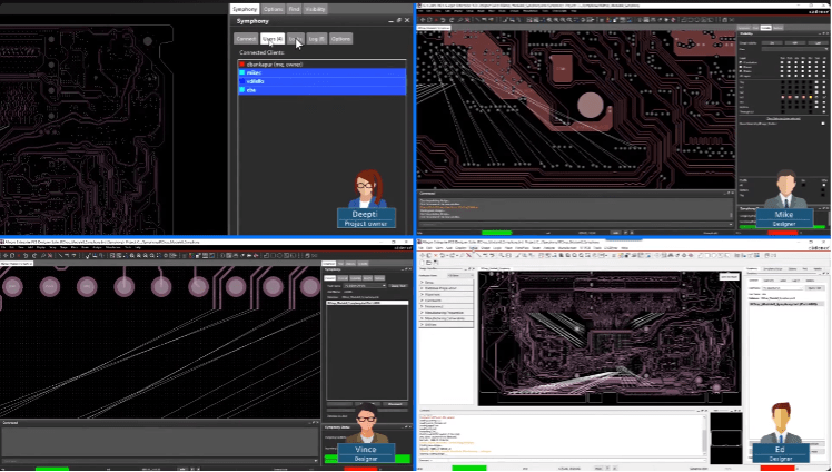
Figure 4. This is a screen grab of a multi-user design environment in Allegro X. Each user can work on different sections of the board in parallel to get designs completed earlier. . As a human, I have a knack for length-matching; not sure if that’s universal. Image Credit: Cadence
With the process limits of this approach in mind, the key players who are creating enormous printed circuit boards will conduct a fully networked approach to the design. A team of designers can combine effort in real time with a single networked database.
There is a certain mojo that goes along with on-line role playing games. People with similar personality defects form bonds while going through video game battles against space monsters or whatever. That kind of “solve it to win” scenario can also be found when three people are distilling strategy into tactics that solve a printed circuit board with “a million” pins.
Having a few subject matter experts in your corner sounds like a good deal.