Tolerances and Dimensions Pertaining to PCB Fabrication
When it comes to coloring in the fabrication drawing, the way in which we provide the data creates the space that the fabricator has to fill. For each datapoint, there is a least material condition (LMC), a maximum material condition (MMC), and a nominal. Process variation is allowed between the two extremes and rejected when it is outside of the envelope.
The nominal value is typically at the mid-point between those two extremes. A typical feature will be expressed with the nominal value and an implied tolerance. The “implied” tolerance is usually stated in the title block or the fabrication notes. The number of digits on the right side of the dimension can be used to assign the tolerance. For instance, 10.0 mm would give us 10 +/- 0.4 while 10.00 mm would allow a feature size of 10 +/- 0.13.
Variations from this process would get their specific tolerance along with the nominal value. There is another method called Limit Dimensions where the minimum and maximum are given but no nominal value is noted. The fabricator is likely to seek the middle ground between min and max to allow for normal process distribution. It’s also possible to use different tolerances for plus and minus. A dimension like 25 +0.10/-0.00 would likely be interpreted as 25.05 +/-0.05 which is why I do not recommend “unilateral tolerances".
Datum Dimensions: Quick, Compact, and Easy
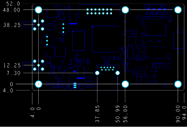
The simplest way to complete the fabrication drawing’s dimensional requirements is to assign a 0.0 location to a feature and base all of the following dimensions on that single datum. Colocating the system origin and the dimensions will simplify the task. From there, the coordinates of the features will match the numbers in the dimensions.

Figure 1. Using the board origin as the datum for the dimensions is good when you start at a hole that is part of a pattern of mounting/tooling holes. Dimension values correspond with the XY position of the hole or other feature. The board edge can be more of a tolerance issue since V-score and mouse-bite processes are not as precise as drilling holes. Image Credit: Author
While a board edge makes sense for most cases, I would use a mounting hole or a tooling hole as the datum for the system and the datum dimensions. Oftentimes, aligning the bolt pattern is more important than a tight tolerance on the edges of the PCB. I’ve heard the argument that the processes are all automated and that the drilling and milling machines use the nominal values for their tool paths anyway.
ANSI Standard Dimensioning (ASME Y14.5)
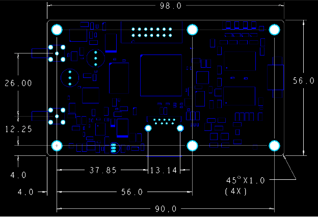
I still believe that some dimensions require more precision than others. The stated purpose of a fabrication drawing is as an inspection document. The traditional dimensions are more flexible in that regard. Using the method above, we can control the pitch between two mounting holes as a function of each hole’s distance from the datum. That’s two separate measurements, each with its own degree of freedom. A direct measurement only allows the implied or stated tolerance rather than an accumulation of tolerances.

Figure 2. This is ANSI ANSI-style dimensions. The tolerance stackup is almost all the same as Figure 1, except for two holes that are chain-dimensioned in order to control their interrelationship. The overall board dimensions set above and to the right of the outline are handy for quotation purposes. Image Credit: Author
Geometric Dimensioning and Tolerancing
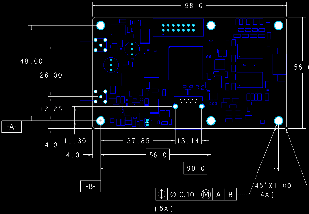
Up until this point, we have been using X and Y coordinates to establish a tolerance defined by a square zone. The size and shape of the zone are determined by the tolerance allowance. We can tighten this up by using a positional tolerance for hole pattern geometry. Instead of the square that allows equal freedom going up, down, and side to side from the nominal, we can define the tolerance as a circle within that square. Cutting off the corners of the tolerance zone allows the same displacement but only from the nominal center outward.

Figure 3. The feature control box at the bottom of this view can have a number of different figures besides the cross-hair symbol for positional tolerance. Other geometric tolerances that are common on PCBs include flatness, runout, parallelism, and profile. Each one creates a zone of acceptable outcomes. Image Credit: Author.
Geometric Dimensioning and Tolerancing also allows us to control flatness and kinds of edges that are not easily dimensioned. One example of this is PCB “mid-mounted” cooling fans. These flat fans use the Bernoulli Principle to move air. The result is that the fan is shaped somewhat like a sectioned nautilus shell, where it has a complex, changing radius. In order to control this outline, there is a Profile specification (Shaped like a D on its side) where the vendor is instructed to follow the arbitrary line or curve with an allowable deviation from the design.
The idea of following the data is built into our process from initial library generation to those emails and phone calls that follow tape-out day. One of the fab notes will (or should) cover layer-to-layer misregistration allowance. It would be rare to actually dimension any of the circuits themselves. You know those antenna people.
Product enablement means taking the image on the screen and turning it into hardware. We want to ensure that the product resembles the artwork as much as possible without over-constraining things. Good judgment looks at the chain linking components, boards, and other subassemblies to products and their end-use.

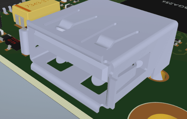
Figure 4. The USB connector pins are the springy type that zig-zag through the board. It’s not quite press-fit, but it does take some force to insert it. The way we yank on those cords is reason enough for a solid build. Image Credit: Author
While the nominal values are important, it’s the tolerances that set the bar for manufacturing. Whether it’s metal thickness in the via barrels or components along the edge, there is almost always a call for a little more wiggle room here and there. We only want to tighten a spec if the process is already failing.
Process control limits are there for a reason. The drama plays out between what the fabricator can do and what the assembly house can’t. A lot of that churn is down in these details. I may not have needed specific dimensions on the USB connector, but the component vendor provided the package details and suggested footprint for a reason. Carrying that over to the fab drawing leaves one less thing to chance.
In the end, this layout didn’t require anything beyond the first effort. Any and all information on the fabrication drawing is subject to being proven out on the actual PCB. Each style uses similar degrees of tolerance but applies them in more specific ways than the one before. What you use will depend on your use case, but the tolerance values generally define the product values.