HDI PCB Design Guidelines
Key Takeaways
- Technology enhances miniaturization and performance, allowing for more complex circuitry in smaller spaces while improving signal integrity and thermal management.
- HDI PCB layout requires attention to material selection, component packaging, routing strategies, and simulation to ensure effective use of space and functionality.
- OrCAD X offers specific tools, such as blind, buried, and micro vias integration, constraint management, and automated via selection, to adhere to HDI guidelines effectively.
HDI Routing in OrCAD X
High-density interconnect (HDI) PCB layout has become the standard for many circuit applications. The reduced space required for the layout allows designers to miniaturize the design, increase the product's functionality, or achieve both of these goals. However, as expected, there are layout details that designers must be aware of when using high-density interconnect technology. Below, we’ve summarized the key HDI PCB design guidelines.
Key HDI PCB Design Guidelines
|
Guideline |
Description |
|---|---|
|
Materials and Processes |
|
|
Components |
|
|
Routing |
|
|
Simulation |
|
|
Vias |
|

Setting physical constraints for Vias for HDI PCB design
High-Density PCB Layout Benefits and Concerns
Printed circuit boards are shrinking in size to build the next generation of compact electronic devices while increasing the amount of functionality they can support. These changes are accomplished by using high pin-count components with pin pitches of 0.5 mm (or less), necessitating trace widths and spaces of 2 mils or 50 microns for their connections. Multiple via technologies, along with advanced fabrication materials and manufacturing processes, define these designs as high-density layouts necessitating the use of HDI PCB design guidelines.
There are many benefits to using high-density interconnect, or HDI, in circuit board design, along with some expected concerns. The improvements in quality and reliability in HDI designs effectively lower their overall costs, making a high-density PCB layout a desirable option. However, there are some concerns that designers need to consider first before jumping into the deep end of the HDI pool.
HDI Advantages
- Miniaturization: Smaller component sizes reduce circuit layout space.
- High-density circuitry: Allows for more circuitry with reduced component spacing.
- Narrow trace width: Increases routing per square inch.
- Diverse via types: Enhances routing space with thru-hole, blind & buried, and microvias.
- Thinner dielectric materials: Improves PCB reliability and reduces board thickness.
- Performance enhancement: Reduces inductance and EMI susceptibility, enhances thermal management, and improves signal integrity

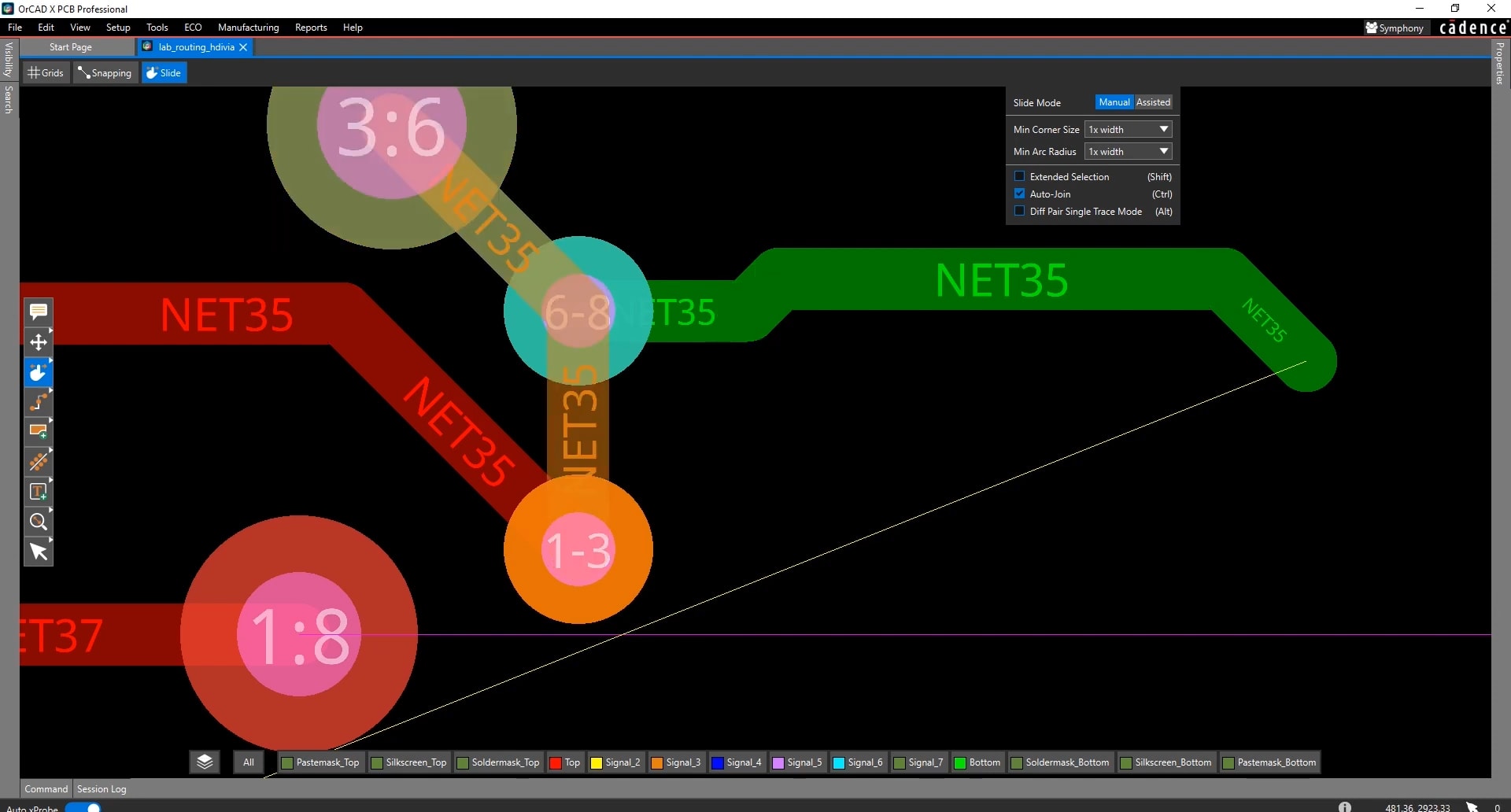
Editing buried and blind vias for HDI routing in OrCAD X.
The following table summarizes the key features, configuration options, and routing techniques available for HDI (High-Density Interconnect) design in OrCAD X. For specifics, see this video.
OrCAD X Rules for HDI: Stacking, Routing, and Vias
|
Category |
Feature / Option |
Description / Usage |
|---|---|---|
|
Via Types |
Micro Vias (Laser) |
Small vias between layers (e.g., 1:2, 2:3). Can be stacked or spaced based on rules. |
|
Core Drilled Vias |
Larger mechanical vias (e.g., 1:8) are used for long spans through core layers. |
|
|
Blind/Buried Vias |
Used for intermediate connections (e.g., blind 1:2, buried 6:7). |
|
|
Via Stacking Rules |
Stacked All |
Vias (e.g., micro to micro) are stacked directly on top of each other. |
|
Coincident Only |
Vias/pads must align exactly with no offset. |
|
|
Edge-to-Edge |
Vias placed with specific spacing, not stacked. |
|
|
Mixed Stacking |
Some layers allow stacked vias, while others use spacing. |
|
|
Constraint Manager Setup |
Via Stacking Rules |
Define stacking rules (e.g., micro to micro, micro to core) per physical rule set. |
|
Same-Net Spacing |
Controls via spacing on the same net (can allow pad overlap or require separation). |
|
|
Hole-to-Hole Constraints |
Used when pad overlap is allowed (takes precedence over pad-to-pad DRCs). |
|
|
Physical Rule Sets |
Assign lists of usable vias for routing (e.g., 1:2, 2:3, 6:7, 7:8, 1:8). |
|
|
Routing Modes |
Working Layer Mode |
Asks the user what destination layer is during routing and automatically selects the correct vias to get there. |
|
Non-Working Layer Mode |
Less granular control; may auto-insert a long via (e.g., 1:8) without stacking logic. |
|
|
Via Control |
Add Connect Mode |
Start routing, and system prompts for next layer transitions. |
|
Double-Click Layer Transition |
System queues the appropriate via stack based on rules and the selected destination layer. |
|
|
Stack Manipulation |
Slide Stack |
Move the entire via stack along the trace path. |
|
Split Stack |
Right-click command that allows peeling off selected vias from a stack for independent manipulation. |
|
|
Excel-like Via Selection |
Select via layers in a cross-section using click-and-drag (like selecting cells in Excel). |
Designers must research potential changes in manufacturing and the resulting new design requirements before starting an HDI design.

OrCAD X has tools specifically designed for HDI PCB design guideline adherence.
How OrCAD X Helps Designers Adhere to HDI Guidelines
OrCAD X supports adherence to HDI guidelines by offering design tools to address the unique challenges of high-density interconnect projects.
OrCAD X Features for HDI
|
OrCAD X Feature |
Description |
How It Helps |
|---|---|---|
|
Blind, Buried, and Micro Vias |
Allows the integration of compact vias that do not traverse the entire board. |
Reduces the need for through-hole vias, enabling more compact, dense layouts. |
|
Constraint Manager |
Enables setting and managing specific design rules tailored to HDI requirements, such as via stacking and spacing. |
Ensures compliance with manufacturing capabilities and adherence to precise HDI guidelines. |
|
Automated Via Selection |
Automates the process of selecting the appropriate via based on routing context and predefined rules. |
Reduces manual errors and speeds up the design process while ensuring adherence to the guidelines. |
|
Stacked Vias Capability |
Provides the ability to create and modify stacked via structures easily. |
Supports intricate layer transitions and optimizes vertical space within multilayer PCBs, crucial for high-density interconnects. |
|
Slide Command for Via Adjustments |
Allows for the splitting or adjusting of via stacks post-placement. |
Facilitates iterative design adjustments crucial for meeting final design requirements and resolving manufacturing challenges. |
|
Interactive Routing Modes |
Enables manual routing guidance while automatically adhering to set constraints for spacing and via usage. |
Allows for fine-tuning of the PCB layout to ensure optimal manufacturability. |
|
Design for Manufacturability (DFM) Checks |
Integrates DFM checks into the design process to identify potential production issues early. |
Helps ensure that the HDI PCB can be manufactured without defects, adhering to design and industry standards. |
Experience the capabilities of the OrCAD X platform firsthand and discover how it can help you adhere to HDI PCB design guidelines. Sign up for the free trial today and take your designs to the next level with our cutting-edge tools and features optimized for HDI compliance.
Leading electronics providers rely on Cadence products to optimize power, space, and energy needs for a wide variety of market applications. To learn more about our innovative solutions, subscribe to our newsletter or our YouTube channel.