How To Use A PCB Stackup Design Tool
Key Takeaways
- The importance of a good layer stackup in your PCB design and understanding the challenges in creating it.
- What designers need to help them create the right layer stackup for their PCB design.
- How Allegro X can help to create the best layer stackup configuration.
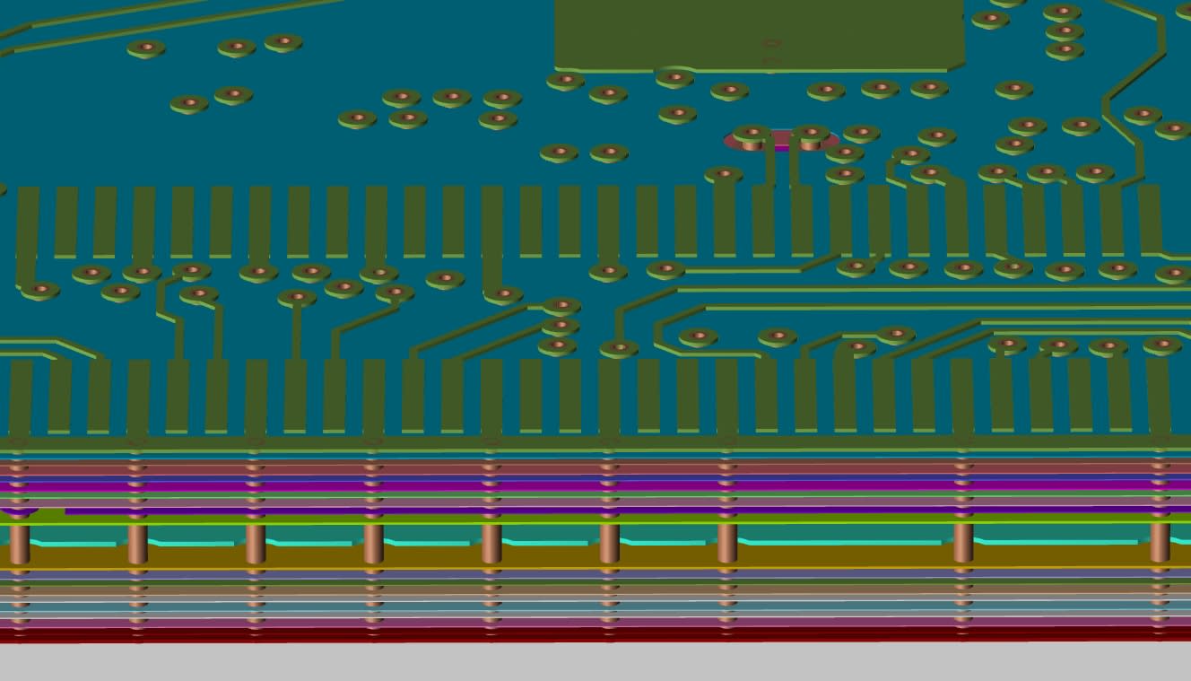
The side and top view of a dense PCB layer stackup
PCB stackup design tools are an essential part of advanced modern day PCB software. Despite these advancements, designers must still meticulously configure the board layer stackup for their designs. We’ll be discussing best practices for configuring stackups using a PCB stackup design tool software.
Critical PCB Stackup Design Tool Features
|
Feature |
Description |
|
Automated Generators/Wizards |
Tools like the Allegro X board creation wizard allow designers to specify layer counts and configurations, automating the creation of the stackup in the database. |
|
Total Control Over Layer Stackup Details |
Designers can specify conductive and dielectric board materials, values, tolerances, and layer arrangements to set up layout parameters. |
|
Integration with Industry Knowledge |
Encourages designers to collaborate with PCB contract manufacturers (CMs) to get accurate information for creating board layer stackups, leveraging manufacturers' expertise. |
|
Bi-Directional Communication with CMs |
Tools like Allegro X PCB Designer enable bi-directional communication with CMs using the IPC-2581 format, facilitating the exchange of board layer stackup information. |
|
Material and Process Familiarity |
Emphasizes the importance of understanding materials and processes, encouraging designers to develop relationships with CMs for better stackup creation. |
|
Advanced Fabrication Materials |
Necessary for high-speed, high-power, or harsh environment boards; can alter transmission line characteristics, requiring changes in layer stackup. |
|
Layer Addition for Enhanced Performance |
Additional layers can provide isolated controlled impedance routing, differential pair routing, microstrip and stripline configurations, and extra plane layers for power and ground nets. |
|
Flexibility in Configuration |
Allows designers to fine-tune board materials, dielectric constants, layer names, functions, and widths to ensure proper configuration for controlled impedance routing. |
|
Time-to-Market Pressure |
Tools help designers meet the intense pressure to quickly get products to market, completing boards rapidly and error-free. |
|
User-Friendly Interface |
Despite the complexity of the tools, efforts are made to enhance user-friendliness, reducing inefficiency and frustration during the design process. |
How Stackup Affects Your PCB Design
The number of layers in a PCB used to be directly related to the number of nets needing routing. As circuitry requirements grew, so did the component and net counts, along with the complexity and pin count of active components. This led to narrower traces or more layers, both increasing manufacturing costs.
As component and net counts rose, so did electrical performance specifications. Designers found that while six layers were necessary to route a four-layer board, eight layers were needed for required performance. Using a PCB stackup design tool for additional layers provided:
- Isolated controlled impedance routing.
- Differential pair routing on fewer layers.
- Microstrip and stripline configurations.
- Extra plane layers for power and ground nets.
With evolving circuit board capabilities, advanced fabrication materials became necessary, especially for high-speed, high-power, or harsh environment boards. These materials can alter transmission line characteristics, requiring changes in layer stackup.
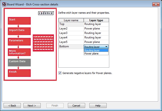
Adding in the board stackup layers into a PCB board outline creation wizard
Layer Stackup Creation Assistance That Helps
There is a lot that PCB CAD tools can do to help the layout designer create and configure board layer stackups.
- The first is incorporating automated generators or wizards like what is pictured above, allowing designers to specify layer counts and configurations for the stackup while the tools do the heavy lifting of creating it in the database.
- The next would be to give the designer total control over the layer stackup details including the ability to specify conductive and dielectric board materials. The designer should be able to specify values and tolerances as well as configure how the layers should be arranged when they set up the parameters of the layout.
- Develop relationships with their PCB contract manufacturers in order to get accurate information for creating their board layer stackups. Manufacturers have been doing this job for years and years, and they are very good at it. Layout designers should be encouraged to engage early on with their PCB CMs in order to have the correct layer stackup before they begin their PCB design.
- Being able to merge the tools with the industrial knowledge of the contract manufacturers would be the best of both worlds. Here is where EDA vendors like Cadence have made real strides with the Allegro X PCB Designer system.
Allegro X provides the capabilities for designers to communicate bi-directionally with participating manufacturers in order to exchange board layer stackup information through the IPC-2581 format. Using the Allegro X PCB stackup design tool, designers can receive stackup information directly from the CM and then send them fabrication and assembly data for manufacturing.
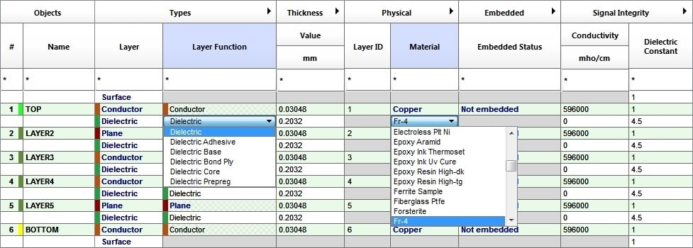
Specifying the dielectric materials in a PCB layer stackup
Using the PCB Stackup Creation Utilities in Your PCB Design Tools
Allegro X is a full-featured design tool that can take your design from schematic all the way through layout. In the picture above, you can see the six-layer board stackup that was generated automatically using a PCB stackup design tool known as the Allegro X board creation wizard. Notice that the values are all generic with a couple of the pull-down menus displayed to show the board dielectric material options that are available for the designer to choose from.
In the picture below, the layer stackup has been fully completed. Additional layers have been added, including silkscreen, solder paste, and solder mask. Also, layer names, functions, and widths have been added, as well as fine-tuning for the board materials and dielectric constants. Now that these layers have been fully defined, they are properly configured to work with the rest of the functionality in Allegro X PCB Designer to calculate controlled impedance routing and other design data.
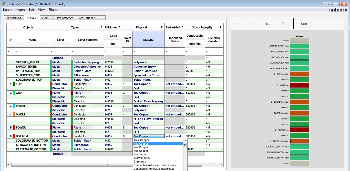
The Cross-Section Editor in Cadence Allegro
How to Create a Stackup in Allegro X
|
Step |
Action |
Reasoning |
|
1 |
Launch Cross Section Editor |
Access the tools necessary to define and modify stackups. This can be done from the icon, typing "X section" at the command line, or using the setup cross-section menu command. |
|
2 |
Enable Multiple Stackups Mode |
Allows for the creation and management of multiple stackups within a single design, essential for complex designs with varying requirements. |
|
3 |
Create New Stackup |
Use the "Add Stackup" button or "+" tab to create a new stackup. This action initiates the process of defining a new set of layers. |
|
4 |
Fill in Stackup Form |
Name the new stackup and select "All layers excluded from stackup." Starting with no layers ensures you only add the necessary ones, preventing unwanted layers from being included by default. |
|
5 |
Add Layers to Stackup |
Manually select and add layers to the new stackup. Customizing the stackup according to the design requirements, such as material, thickness, and layer order, ensures precision. |
|
6 |
Repeat Layer Addition |
Add additional layers as needed to complete the stackup. Ensures all necessary layers are included for the stackup to function correctly in the design. Use the copy function to replicate an existing stackup when needed. Saves time and ensures consistency across similar stackups. |
|
7 |
Verify Stackup Details |
Check the total number of layers and other details for each stackup by selecting the respective tabs. Confirms that the stackups are correctly configured and complete. |
|
8 |
Update Cross Section Display |
Ensure the cross-section editor display reflects the changes made to the stackups. Visual confirmation of the stackup configurations helps verify correctness and aids in troubleshooting. |
|
9 |
Setup Default Materials |
Define default materials in the materials cmx file and layer materials XML file. Ensures consistency and compliance with design standards. |
|
10 |
Check Electrical Properties |
Verify electrical properties like differential spacing and signal integrity. Ensures the design meets electrical performance requirements. |
|
11 |
Add Mask Layers |
Add additional layers such as solder masks, silkscreens, adhesives, and stiffeners. Completes the stackup configuration to include all necessary layers for both rigid and flexible parts of the PCB. |
With advanced PCB stackup design tools like Cadence Allegro X, you will have the capabilities that you need to fully setup and configure your design for layout. To read more about this process, take a look at this E-book.
Leading electronics providers rely on Cadence products to optimize power, space, and energy needs for a wide variety of market applications. To learn more about our innovative solutions, talk to our team of experts or subscribe to our YouTube channel.