Solder Paste and Stencil Considerations For Double-Sided Printed Circuit Boards
Thought provoking questions keep coming my way and then it’s down the old rabbit hole. So, it goes something like this. “How do we integrate so many different parts in such a small PCB area?” The answer is a little deeper than the geometry of Tetris but that’s a good illustration of packing the available space. This, of course, starts with the CAD symbol library and manifests in the assembly yields at the factory. We have to connect those dots.
…unlikely that every device on the board will be able to meet that preference
Once the PCB logic is sufficiently captured, placement studies can start. It’s important to pay attention to spacing and orientation of the components. The interrelationships of neighboring parts can affect the solderability of the overall PCB. The assemblers like to see a consistent rotation of the components and an even distribution across the board.
It’s unlikely that every device on the board will be able to meet that preference. The electrical performance is going to take priority in a number of cases, particularly with analog designs. That said, you can still pick an orientation that suits most of the components. The similarity will inform the Manufacturing Engineer as to how the board should travel along the placement machinery and guide the soldering process.
Creating an A/B Flip Panel
Manufacturing may also drive the assembly sub-panel geometry. They will look at how the majority of the parts are rotated and send the board through the process so that most passive components go through broadside to the direction of travel. This would have both leads being soldered at the same time rather than sequentially. The effort helps reduce the infamous tombstoning defect.

One XY pick and place file and one solder paste stencil suffice for both sides of the board in one go. Aside from saving on a stencil, the time it takes to populate one side of the panel is exactly the same as populating the other side. Quite often a board ends up with more parts on one side than the other, creating an imbalance of the time it takes for each side of the board. With half of the boards “up” and the other half “down”, the time and set-up for each operation is the same.
One of the key parameters of an A/B flip subpanel is the weight of the components. Heavy parts are not so good at staying attached when they are on the underside. Glue can be used but it’s a cost and process subject to cosmetic issues. Ungluing can be a pain when it comes to rework. More likely, the heavy part will negate the option so all of the boards will be empaneled with the same side up.
In any case, the sub-panel will support assembly with tooling holes and fiducial marks on both sides. The discarded area of the subpanel may also have a test coupon or an arrow that shows which way to handle the panel in the fixture. Don’t make these people have to guess.
Implementing Soldermask Defined Lands
There is a general rule of thumb where the paste stencil opening is equivalent to the copper area of the pad. That would generally be two mils smaller than the soldermask opening. That would hold true until the soldermask is all that’s left to define the pad.
When the ambient copper floods over a pad, it becomes mask-defined by definition. When this is the case, only the paste stencil is left to represent the vestigial pad that was consumed by the copper flood. The soldermask has to shrink to the original pad size matching with the paste size for a repeatable solder joint.
One of the main reasons for soldermask defined lands is accommodating fine pitch devices. The must-have that defines the process is the minimum web that can be laid down between two pads. If the minimum web is wide enough to paint the entire gap between the pads, then it’s clear that you have to use soldermask defined lands. The soldermask web is also relevant to the paste stencil in that there is a minimum width of material required between stencil apertures.
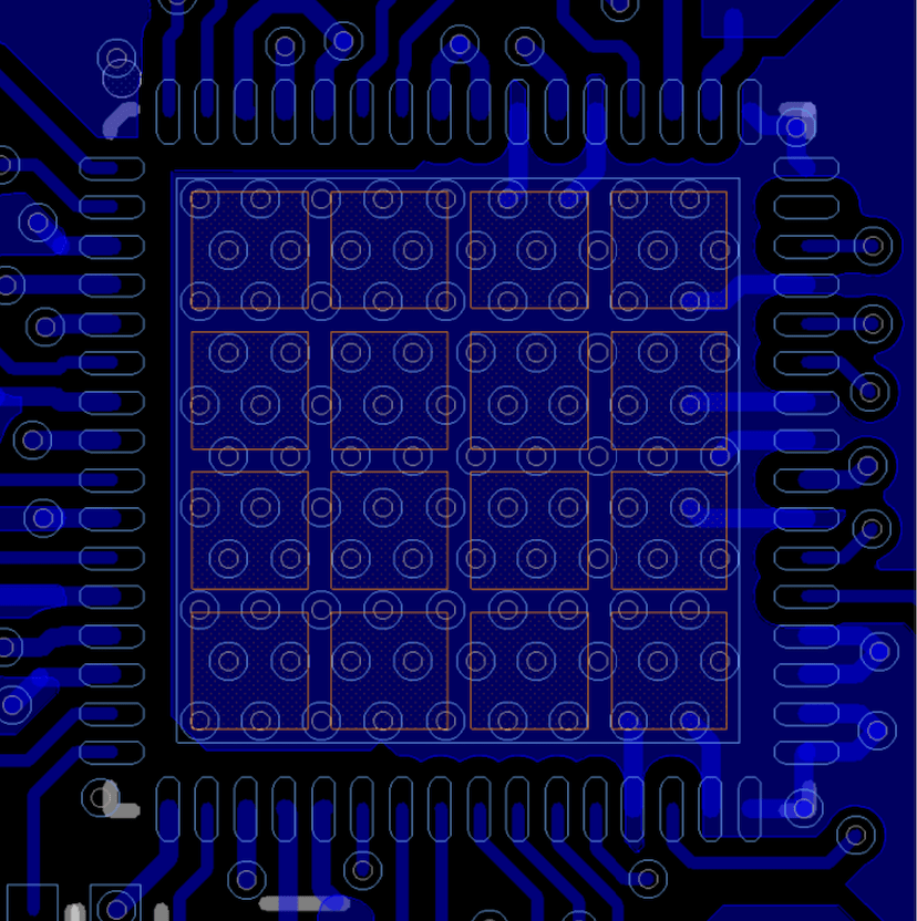
Figure 2. Fine pitch devices may require solder mask defined lands rather than non-soldermask defined lands so as to get a proper laydown of mask between the pins. The GND paddle paste mask is broken into 16 squares to calibrate the amount of solder. Image Credit: Author
Gang relief is usually a last resort since the solder dam is what helps keep each solder joint in its own little world. When you don’t have the mask between pads, the amount of paste has to be decreased to starve out the tendency for solder to create bridges from one pad to the next during reflow. An exception to that is where there are pins that do not get soldered. Edge connectors and press-fit connectors fit this profile.
The Ever-Shrinking Footprints In The Name Of Progress
As the package size shrinks, the integrity of the pad and the paste opening become critical parameters affecting assembly yields. The paste apertures as well as the actual solderable land may need to be more organic than the datasheet suggests. Rounding off the corners of the pad is becoming more common.
When it comes to the 01005 size passive components, the footprint could end up with D shaped pads with a full arc around the toe filet. Further, it may be mandatory to fan-out the pads with a specific width line that extends from the center of the pad. The pad would have non-solder mask defined lands. A little extra mask would fill where the trace exits the pad to make that spot mask defined.
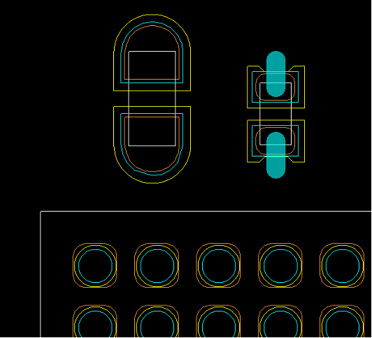
Figure 3. The differences between 0201 and 01005 can be profound. The footprint on the right is for an 0201 part while the left shows a suggested footprint for an 01005 size. Note that the solder mask opening tucks in where the predetermined fan-out traces run. So The 01005 pads are non-solder mask defined except where the trace is routed. The mask expansion is reduced from 50 to 37 microns for the smaller part. Launching a trace from the side of the pad would require an alternate footprint that adjusts the mask. Image Credit: Author
There are other potential ways that the paste stencil openings would not match the metal layer. The so-called home plate pad bevels the stencil to reduce the amount of paste under the gap between the pads. Another approach rotates the 5-sided home plate such that it points away from the center of the part. That one plays out more like the D shaped pads mentioned above. It comes down to what type of solder defect is showing up the most.
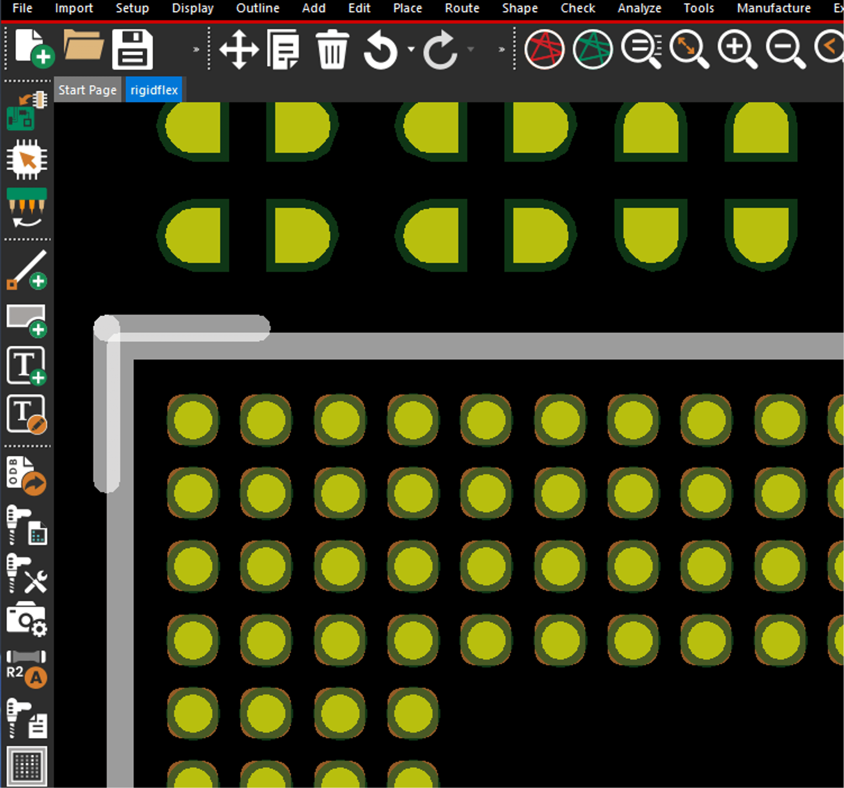
Figure 4. With yellow for metal, green for mask and gold for the stencil, this 0.4 mm pitch BGA footprint is an example of over-printing the solder paste. The reflow process will draw the extra paste into the joint. Meanwhile, the 0201 package makes a good complement to the 0.4 mm class of devices. You will often find them scattered under the BGA as the typical double sided use-case. Image Credit: Author
Time = Money
My first ECAD job had us Designers buying their paste stencils from the same local vendor. One day, our Manager pulled me aside and asked why I paid $140 for a stencil when everyone else paid $175 for theirs. The difference was that I did not select the expedited schedule option.
When the factory is right down stairs or in the next building, the tactical aspects of the PCB enablement shine brighter. In some cases it’s probably better to have a buffer between engineering and the actual production line. Engineering changes have to be vetted in some way before taking effect. When a solder defect is holding up progress, finding the root cause and delivering a workable solution should be a top concern in any case.
The price is often the key metric for consumer goods. That aspect really tilts the table towards off-shore manufacturing where the feedback loop is measured in time-zones. We don’t feel the pulse of a fab shop halfway around the world. This only sharpens the focus on the pre-production data from the assembly team. Make their problems your problems and, hopefully, there will be no further problems.
Reacting To Unforeseen Issues Is A Day In The Life On The Assembly Line
Even with the best laid plans, solder defects can find their way into a board. We have pre-production cycles in order to help resolve these issues. There are tell-tale signs of not enough or too much paste in the mix. Individual apertures can be modified to solve defects related to too much solder. Typical clues for excess solder will be solder balls, bridging, dross or head-on-pillow defects. Insufficient solder will manifest in pinholes, non-wetting and disturbed solder joints.
This is one of the reasons that we have pilot programs
Assembly yields from the above defects should be analyzed at the first opportunity. Often, a global edit to the offending padstack is the most effective remedy. When it’s too late for that, you have to look at the thickness of the stencil and the geometry of the openings. The volume of the solder can be increased by over-printing beyond the existing pads. It can be likewise decreased with a smaller opening or by creating a windowpane of four separate openings for a large copper pad. Figure 2 details an array of 16 windows as a jumping-off point.
Solder paste can be procured in large containers for mass production but also comes in applicators similar to a syringe or turkey baster for depositing it by hand. Scaling up and gaining the precision necessary for fine-pitch devices can also be done with refrigerator sized machines that apply the paste robotically.
Robots have to be programmed to do each type of board and they cost big money. Wait for them to be synthesized on a pad-by-pad basis using the AI with the right set of prompts. With enough equipment, you might get away from using paste stencils altogether.
In the factory, dispensing solder paste is not as fast as using a stencil. On the plus side, they are more adaptable to updates when the board gets a minor placement revision. It’s a capital cost that would allow the manufacturer to put a few people into better positions.
Reflow temperatures will vary with different solder paste formulas.The paste itself can be more or less granular in composition. The finer grain will get into the smaller openings better. More than likely there are reduction of hazardous substance agreements in place. That will narrow the field a little. You start with the normal formula for SAC305 solder and make adjustments if there are trending solder defects. This is one of the reasons that we have pilot programs.
The board is a fixed cost that is usually a fair portion of the overall bill of materials all by itself. Add in all of the bits and pieces of the assembly and note that you are now deeper into the schedule as well as the production cost curve. This is why knowing the intricacies of the assembly process is one more key to delivering a profitable program.