Advanced PCB Design Techniques: OrCAD X Routing and Placement
Key Takeaways
-
Techniques like HDI, differential pair routing, and impedance control are essential for managing complex PCB designs.
-
Effective component placement, particularly for high-pin count devices, is crucial for maintaining signal integrity and managing routing complexity.
-
OrCAD X offers real-time feedback, via optimization, and design rule checking to simplify the design process and ensure adherence to constraints.

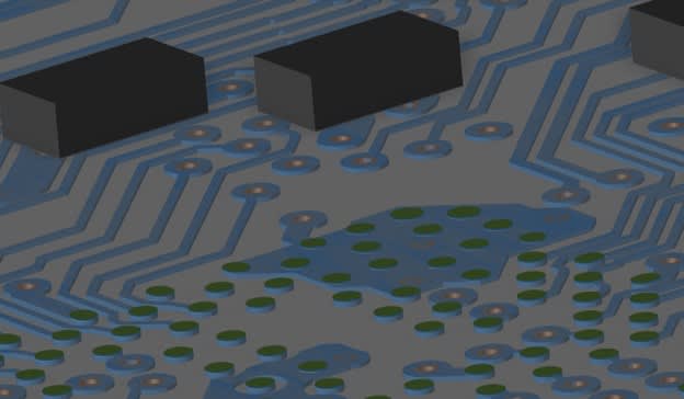
Screenshot of OrCAD PCB Designer showing complex internal layer routing
For years, PCB designers have relied on a mix of automated and manual routing tools to create circuit board traces, with many favoring the manual approach using interactive tools. This tried-and-true method has served well, but as circuit board technology advances to meet new challenges, designers must adapt. As designs grow more complex, the need for advanced routing techniques becomes critical. Fortunately, there are already innovative advanced PCB design techniques, from routing to placement, all available to help designers navigate these new demands, and we will explore some of them here.
Advanced PCB Design Techniques for Emerging Technologies
Advanced PCB design techniques are becoming increasingly essential across various fields in electronics. Evolving processor and memory technologies, such as those found in larger BGA packages with growing pin counts, require precise routing to ensure successful trace connections. Similarly, advancements in memory components demand new methodologies for DDR routing to manage double-data rate connectivity.
To succeed in these evolving areas, PCB designers must familiarize themselves with these advanced routing strategies discussed further below. Understanding the specific needs of medical IoT circuits, mastering BGA trace routing, and getting comfortable with DDR techniques are key steps. Fortunately, there is a wealth of information available to help designers navigate these challenges, some of which we will explore here.

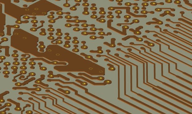
Escape routing for BGA pads using advanced PCB design tools
PCB Trace Routing Tips and Recommendations
When tackling advanced PCB routing, it’s essential to prioritize several key guidelines to ensure a successful design.
-
Start by setting up clear design constraints before beginning the routing process, as this will guide all subsequent decisions and prevent costly revisions.
-
Use High-Density Interconnect (HDI) techniques to maximize board space, especially when dealing with complex, multilayer boards.
-
Differential pair routing is crucial for maintaining signal integrity, so ensure that these pairs are routed with consistent spacing and equal lengths to minimize noise.
-
Implement impedance-controlled routing for high-speed signals, carefully managing trace width and spacing to maintain the desired impedance.
-
Length tuning is another vital step, particularly in high-speed designs, where precise control over trace lengths is necessary to meet timing requirements.
-
Utilize via optimization by selecting the appropriate via types and carefully managing their placement to avoid unnecessary signal degradation or manufacturing issues.
-
Lastly, consider using assisted routing modes for dense areas to maintain adherence to design rules while streamlining the routing process.
How OrCAD X Enables Advanced PCB Routing Techniques
|
Routing Technique |
OrCAD X Feature |
Description |
|
High-Density Interconnect (HDI) Routing |
Constraint Manager, Micro Via Support |
|
|
Differential Pair Routing |
Real-time Constraint-driven Feedback, Differential Pair Setup |
|
|
Grid Based Routing |
Grid and Snapping Configuration |
|
|
Impedance Controlled Routing |
Add Connect Command, Impedance Profiles |
|
|
Length Tuning and Delay Matching |
Delay Tuner, Graphical Heads-Up Display |
|
|
Auto Routing with Assisted Mode |
Assisted Route Mode, Hug and Shove Options |
|
|
Routing with Via Optimization |
Slide Command, Stack Via Management |
|
Routing Architecture with Medical IoT Circuits
The Internet of Things (IoT) has transformed our daily lives, connecting everything from refrigerators to lighting, and now extends to medical devices that monitor and maintain our health. For PCB designers, this shift brings greater challenges and responsibilities, as the stakes are much higher in medical applications. A malfunction in an implanted device could have severe consequences, making it crucial for designers to create flawless, reliable circuit boards for these life-critical devices. If you’d like to learn more about this subject, read about some of the medical IoT connection considerations here.
Routing Traces Out of BGA Packages
As computing power demands rise, BGA packages are becoming larger with more pins, as vendors decrease pin-pitch to add functionality. Designers face the challenge of routing these increasingly complex parts, but there are many resources available to guide them. Key tips include organizing signal paths and using diagonally routed escape patterns for larger BGAs. If you would like additional information on routing BGA packages, read about it here.
Considerations for DDR Routing Techniques
Routing memory circuitry, particularly for DDR memory, is one of the most precise tasks in PCB design, requiring trace lengths to match for accurate data capture on the clock signal's edges. This demands careful component placement and room for routing connections, often involving trace tuning to ensure length matching. Designers must also plan for specific routing patterns tailored to the memory circuit's needs.There’s a lot for the designer to understand in memory routing, and you can read more about DDR routing techniques here.

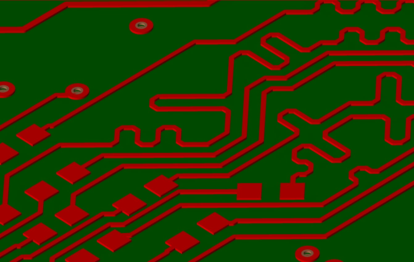
PCB design tools with advanced functionality can help to create routing like this
Advanced PCB Layout Techniques
Effective PCB layout and placement are foundational to achieving a high-performing and manufacturable design. Thoughtful component placement is crucial, as it directly impacts signal integrity, thermal management, and the overall footprint of the board.
-
Grouping components by function and proximity to related signals can minimize trace lengths, reduce noise, and improve electromagnetic compatibility.
-
Optimizing the placement of high-pin count devices like BGAs is essential to manage routing complexity, especially when dealing with dense designs.
-
Careful consideration of power and ground planes, ensuring that they are well-positioned to minimize impedance and support efficient current paths, is also key.
-
Lastly, employing strategies such as fanouts, via arrays, and shielding techniques can further enhance signal integrity and simplify routing.
These best practices in layout and placement are integral to the creation of robust and reliable PCBs that meet design specifications and manufacturing requirements.
OrCAD X Features for Layout and Placement
|
PCB Layout and Design Task |
OrCAD X Feature |
Description |
|
Component Placement Optimization |
Import/Export Placement |
Allows designers to export and import component placements as a CSV file, enabling consistent placement across different designs or tools. |
|
High-Pin Count Device Management |
Fanout Strategies, Visual Graphics |
Provides visual tools and strategies to test and optimize fanout patterns for devices like BGAs, making routing more manageable. |
|
Design Rule Checking (DRC) |
Interactive DRC Overview, Slide Command |
Enables real-time DRC monitoring and easy adjustment of traces to resolve violations during layout and placement. |
|
Power and Ground Plane Optimization |
Add Plane Command, Power Net Assignment |
Simplifies the process of adding and managing power and ground planes, ensuring optimal placement for signal integrity and thermal management. |
|
Visibility and Design Management |
Stipple Pattern, User-Defined Views |
Enhances design visibility with stipple patterns and customizable view settings, allowing for easier management of complex designs. |
|
Assembly-Friendly Component Spacing |
Ability to Set DFA Rules |
Allows setup of Design for Assembly (DFA) rules like package-to-package spacing, ensuring components are spaced correctly for automated assembly processes like pick-and-place, or manual processes where larger clearances are required. DFA rules also support varied spacing for different component types and classifications (e.g., connectors, chips, ICs), simplifying assembly and reducing errors. |

Trace tuning to control the length of PCB routing are essential for DDR routing
Streamline Your Workflow with OrCAD X Advanced PCB Design Techniques
Advanced PCB design techniques are essential for creating high-performance, reliable electronic products. Designers can leverage these techniques to optimize component placement, manage signal integrity, and streamline routing, ensuring their functional and manufacturable designs. To explore how Cadence can elevate your PCB design process, visit the PCB Design and Analysis Software page and learn more about OrCAD X.
Leading electronics providers rely on Cadence products to optimize power, space, and energy needs for a wide variety of market applications. To learn more about our innovative solutions, talk to our team of experts or subscribe to our YouTube channel.