Editing PCB Components in OrCAD X
Key Takeaways
-
Modify PCB component symbols in OrCAD X Capture using the Symbol Editor to adjust pins, text, and shape.
-
Assign alternate footprints in OrCAD X by editing properties and syncing updates with the PCB layout.
-
Place and group components efficiently using the Component Explorer and grouping features in OrCAD X Capture and PCB Editor.
How to edit a PCB component symbol in OrCAD X
Editing PCB components can be important to create accurate and functional circuit designs in OrCAD X. Whether you're adjusting component symbols, assigning alternate footprints, or organizing groups within your schematic or PCB layout, OrCAD X provides powerful tools to streamline the process. Below, we’ll cover tasks related to editing PCB components, including symbols, footprints, placing components, and grouping components.
Editing PCB Component Symbols in OrCAD X
|
Step |
Details |
|
Open OrCAD X Capture |
Select your desired part in the schematic. |
|
Launch the Symbol Editor |
Right-click the component and select Edit Part. |
|
Modify the Graphic |
Add, delete, or reposition pins; adjust the symbol’s shape; and modify text attributes (like the reference designator placeholder). |
|
Save and Update |
Save the symbol and update your schematic so that the new version is used. |
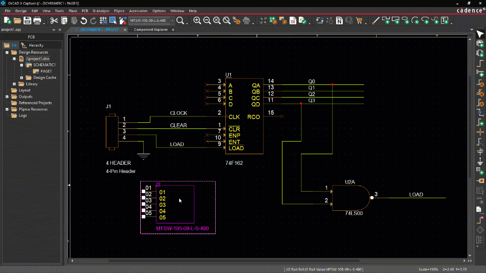
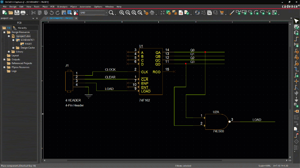
How to Place Components in OrCAD X Using the Component Explorer
To add a component to your schematic you can use the Component Explorer, which gives you access to more than thousands of online parts through various providers’ component libraries.
-
Click the "Place Component" icon in the toolbar.
-
Navigate to "Place → Component" in the menu.
-
Press the "M" key on your keyboard.
The Component Explorer simplifies part selection and management by enabling you to:
-
Browse Cadence’s extensive component libraries.
-
Log in to access the SamacSys part libraries (note: separate credentials are required for Ultra Librarian and SnapMagic).
-
Use keyword searches to quickly locate and download components from Cadence’s content partners.
-
Access a comprehensive collection of parts, including symbols, datasheets, footprints, and 3D models.
How to easily place components in OrCAD X
Setting Alternate PCB Component Footprint in OrCAD X
For editing PCB components with alternate footprints available, follow these steps:
Setting alternate footprints in OrCAD X Capture
Verify the Downloaded Footprints Are Available
-
Open File Explorer:
-
Type %home% in the address bar to open your home folder.
Locate the Downloaded Footprint Files:
-
Browse to:
cdssetup\orcad_capture\<version>\downloaded_parts\allegropcb -
Find the most recent files. For example, you might see “PW20” as the main footprint and “PW20-L” and “PW20-M” as secondary footprints.
Close File Explorer.
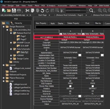
Assign Alternate Footprints via Properties
-
Edit Properties for One Component Instance:
-
Back in OrCAD X Capture, right-click an instance of the newly placed component and select Edit Properties.
-
The Property Editor tab will open.
Add a New Property for Alternate Footprints:
-
Click New Property to open the Add New Property window.
-
Enter the property name: ALT_SYMBOLS
-
For the value, enter:
PW20-M;PW20-L -
Click OK, then Apply, and close the Property Editor tab.
Sync the Changes to the PCB
-
Save the Design:
-
In the Project Hierarchy, select the design file.
-
Go to File > Save to save the whole design.
Update the PCB Layout:
-
Select PCB > Update Layout from the menu.
-
In the Update Layout window, click Sync to apply the changes.
-
This action will open OrCAD X Presto.
-
Select the appropriate license and click OK.
-
OrCAD X Presto will show a Change Report. Close the report.
Finalize the Update:
-
Go to File > Save to save the changes.
-
If prompted to overwrite the design, click Yes.
Verify the Alternate Footprints in the PCB
-
Place the Components on the PCB:
-
Right-click the Move Mode in the toolbar and select Place.
-
In the Placement widget, select Series to place one component at a time.
-
Click the hyperlink for unplaced components in the Properties panel to open the list in the Search panel.
-
Select the components from the list; a red rectangle will appear on the canvas indicating the placement boundary.
-
Click to place the component and press Escape when finished.
Check the Footprint Assignment:
-
Select a placed component.
-
In the Properties panel under General, open the Footprint dropdown.
-
Verify that the additional (alternate) footprints are listed.
-
Choose a footprint from the list to assign it to the component.
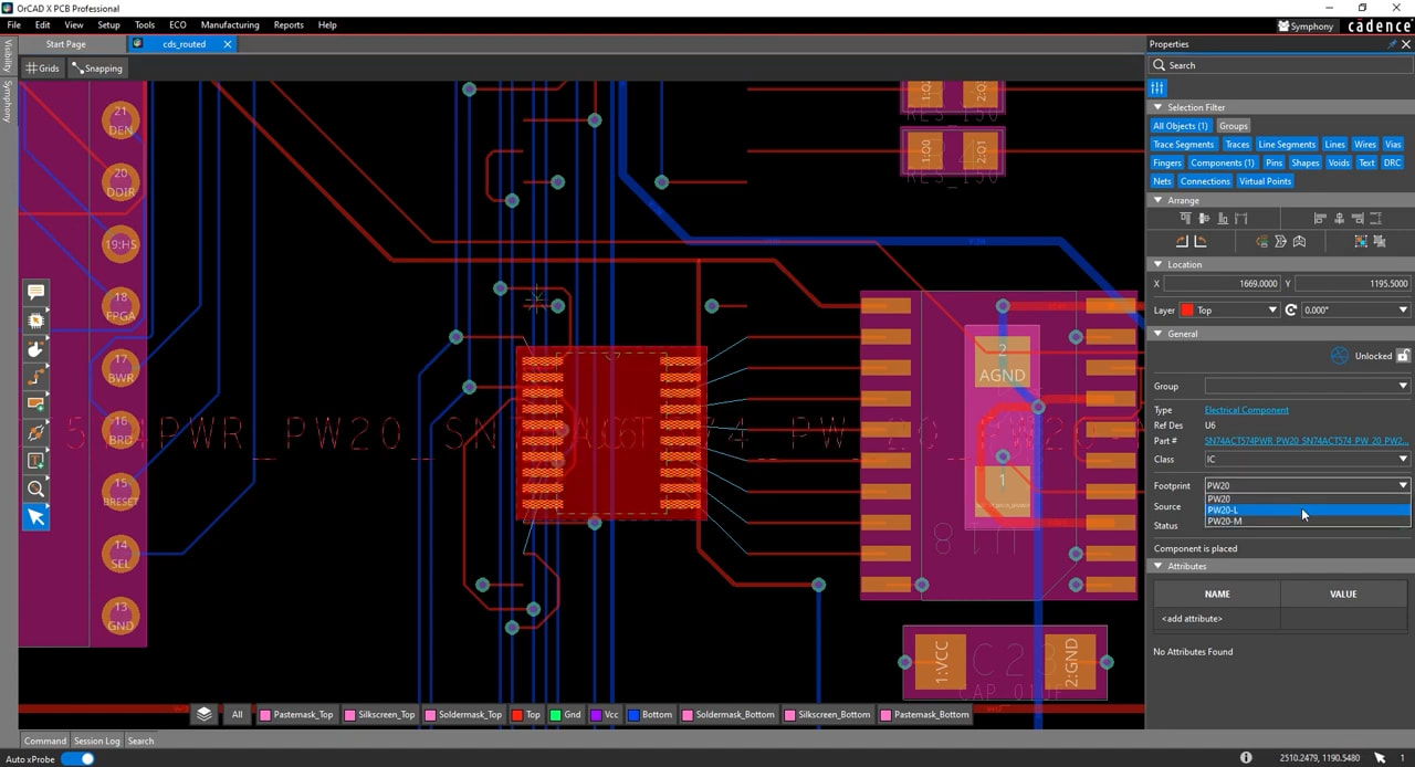
Alternate footprints in the properties panel in OrCAD X Presto
Quick Method of Editing a PCB Footprint
|
Step |
Editing Details |
|
Select and Open the Footprint Editor |
Right-click the component and select Edit Footprint. If the footprint is in your library, it will open automatically. If not, you’ll be prompted to export it from the database into your working directory. |
|
Apply the Changes |
A second OrCAD X Presto window opens in the Footprint Editor while keeping the original layout open. You can: Move pins, adjust place boundaries, add or remove pins, or replace pad stacks. |
|
Save and Update the Layout |
Once edits are complete, go to File > Exit and save the changes. The layout editor will detect the update and prompt you to apply changes, including updating text, removing fanouts, and refreshing pad stacks. |
|
Select the File and Click Open |
Click OK to apply updates to the entire design. Every instance of the footprint in the layout will reflect your changes. |
Grouping Components in Layout/Schematic
Grouping components is useful for logical organization and ensuring that related parts move together. In OrCAD X, there are ways to “group” components both in the schematic capture tool (OrCAD Capture) and in the PCB layout (PCB Editor).
In the Schematic (OrCAD Capture):
-
Selection & Annotation: You can select multiple components (using Shift or Ctrl) and then use the context menu’s “Group” command or simply add a net label/room property to logically group them.
-
Hierarchy: Creating sub-sheets and hierarchical blocks is another method for grouping related symbols.
In the Layout (PCB Editor):
-
Manual Grouping: Select a group of components by dragging a selection box. Then, use the “Group” (or “Lock Group”) command available from the Edit menu or via right-click to ensure that these parts move as one.
-
Filtering: Some versions of OrCAD X allow you to filter and then place or adjust groups by using search features
Editing PCB components in OrCAD X allows you to make sure your schematic and layout accurately convey the information needed. With OrCAD X, you’re able to easily modify every aspect of your design. Learn more about the OrCAD X platform and Cadence’s PCB Design and Analysis Software tools.
Leading electronics providers rely on Cadence products to optimize power, space, and energy needs for a wide variety of market applications. To learn more about our innovative solutions, talk to our team of experts or subscribe to our YouTube channel.