Use the OrCAD X Align Components Feature for Better Assemblies
Key Takeaways
-
Aligning components allows designers to quickly organize large groups of components or circuit blocks, accelerating the overall layout timeline.
-
Alignment guides make it easier for designers to eyeball alignment when free-placing components.
-
Additional placement tools found in the Properties support further layout optimization.
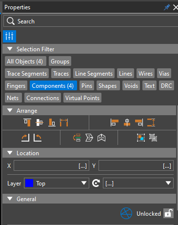
The OrCAD X align components feature can be found underneath the Properties panel when selecting multiple components.
An assembled PCB can resemble dense urban planning with its narrow routing channels, repeated circuit blocks, and taller components that jut out from the board like a skyscraper. Designers must be sure their placement optimizes the board space available before investing considerable time into routing, especially in HDI designs where placing all of the board’s components (much less routing them) is a significant achievement. The OrCAD X align components feature ensures an expeditious placement before routing, creating a ready-for-assembly design.
OrCAD X: Align Components by Axis
|
Horizontal |
Vertical |
|
Align Top - Aligns components by top edge. |
Align Left - Aligns components by left edge. |
|
Align Middle - Aligns components horizontally by midpoint/center/origin. |
Align Middle - Aligns components vertically by midpoint/center/origin. |
|
Align Bottom - Aligns components by bottom edge. |
Align Right - Aligns components by right edge. |
|
Distribute Horizontally* - Equally spaces components horizontally. |
Distribute Vertically* - Equally spaces components vertically. |
* Only available when selecting three or more components.
How to Use the OrCAD X Align Components Feature
Aligning components in OrCAD X is a simple process based on the Move command.
- Start by making sure the Properties panel is visible (users can open it under View > Panels > Properties in the top toolbar if it was closed in a prior session).
- Expand the Selection Filter tab within the Properties panel to select only components.
- Highlight the components in the canvas for alignment by dragging a window.
OrCAD X Presto PCB Editor users can access the Alignment Guides underneath the Snapping tool. When placing manually with Alignment Guides enabled, users will see lines connecting pad centers, component centers, and other notable component elements. Dragging the component in the direction of the Alignment Guides will gently “lock” the component’s movement in the perpendicular direction to ensure the components remain aligned. Dragging the component perpendicular to the Alignment Guide lines will cause them to disappear, ensuring they do not inhibit placement workflow.
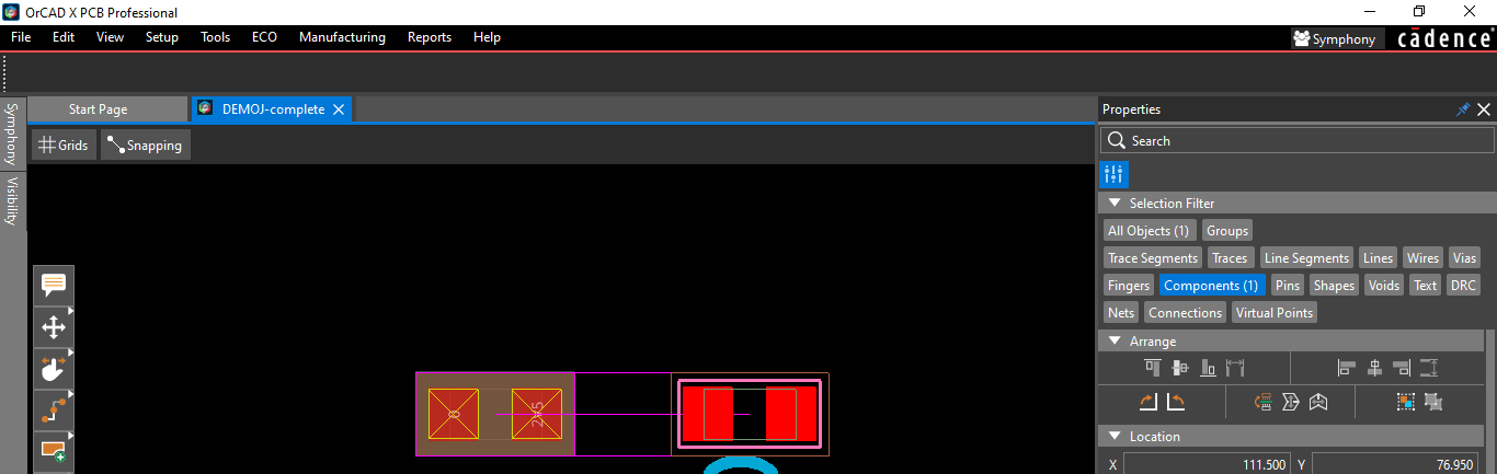
Alignment Guides (lines shown in fuchsia) help designers eyeball alignment during placement.
Additional Placement Organization Tools
After aligning components to fit the board placement needs, users can then lock the placement position with the padlock symbol under the General tab, which will display a closed/locked padlock when the user sets placement (note that users can also lock/unlock objects within the Search panel results). This feature ensures that any components, even those highlighted by the Selection Filter or from Search bar results, remain locked in position until they have been unlocked by the user, preventing accidental movement of components during placement.
Additional features of the Move command in the Properties panel include:
-
Rotate the components to optimize board space usage.
-
Mirror components to the other side of the board (i.e., XY position remains the same, and the component rotates 180 degrees around its vertical axis).
-
Group/ungroup components together. A group is a user-defined object class that shares an association. Users could group all components in a circuit block, making them easier to see during floorplanning and allowing users to manipulate the circuit block singularly with separate Selection Filter options. Note that groups are not limited to just components and can contain multiple different object types.
-
Set the XY position for components, which is helpful for connectors or other components with a defined location in the design document.
Beyond aesthetic preferences (neatness counts!), layout designers know proper placement is conducive to easier routing. Time spent aligning components during placement ensures that nearby traces remain short and direct for the lowest impedance pathway possible. Additionally, manual and automated testing/debugging methods can benefit from an aligned layout that simplifies diagnosis or fixture design.
For routing that spans multiple layers or runs across the top/bottom layer, alignment before via fanout helps ensure the circuit block has enough room for signal breakout from pin-dense components. Additional placement tools, like an easily customizable grid with metric and Imperial units, improve manufacturability by keeping the design on-grid and 1:1 with location between the design environment and assembly equipment.
OrCAD X Align Components Feature: The Solution for an Optimal Board Layout
The OrCAD X align components feature rapidly accelerates placement while minimizing defects in the assembly process. Component alignment contributes to a visually aesthetic board and makes it easier to route – a crucial factor for high-density designs.
With the new OrCAD X platform, design teams can more readily prepare for manufacturing with a powerful and easy-to-use ECAD environment. Interested in learning more? See how Cadence PCB Design and Analysis Software bolsters cutting-edge product development.
Leading electronics providers rely on Cadence products to optimize power, space, and energy needs for a wide variety of market applications. To learn more about our innovative solutions, talk to our team of experts or subscribe to our YouTube channel.