OrCAD X: Next-Gen Circuit Board Design Software
Key Takeaways
-
From the schematic to the layout, OrCAD X combines cutting-edge features with an easy-to-learn interface.
-
Upgrades to Canvas 3D enhance visualization in preparation for MCAD-ECAD system assembly or flex/rigid-flex designs.
-
Live BOM and Live DOC enhance manufacturability by synchronizing the BOM and documentation to real-time updates.

The new OrCAD X Presto PCB Editor combines powerful functionality with an approachable UI.
The challenges of modern circuit design are numerous: reliability and performance are often at odds with one another as circuit density grows. Designers need an all-encompassing solution that can meet the totality of modern-day circuit complexity without overwhelming menus and command lists. Cadence’s new OrCAD X provides design teams with a best-in-class design platform with fully integrated support for every aspect and level of board design, from the single user to the full design team. OrCAD X accelerates layout with a simplified UI for circuit board design software that doesn’t sacrifice power or functionality.
How OrCAD X Improves Design Phase Workflow
|
Schematic |
|
|
BOM and Procurement |
|
|
Layout |
|
|
Documentation |
|
Building Circuits From Schematics
Printed circuit workflow typically follows a process of design, simulation, layout, prototype, test/measure, and revision. As such, software needs to comprise (or at least accommodate) these critical aspects: OrCAD X does so in spades. It begins with OrCAD X Capture CIS for schematic creation, part library management, and netlisting of the design. OrCAD X Capture CIS features a complete part authoring environment that synchronizes with the BOM and provides real-time updates via the new Live BOM functionality for a more supply chain-resilient part selection.
The first step of circuit board design software is creating the schematic. Here, designers will symbolically represent the logical connection between components without concern for physical distance. Since the schematic represents the PCB at a higher level of abstraction than the layout, no physical information is necessary (at this point, any physical demands of the printed circuit belong to the design documents). Engineers and designers only have to concern themselves with the surface-level topology of the circuit – whether component A’s pin 1 connects to component B’s pin 2, not how they connect.

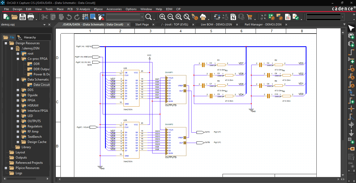
The schematic diagrams within OrCAD X Capture show the logical association between components for the layout.
The schematic symbols must be associated with an accurate footprint to satisfy the electrical pinout of the components found in the assembly. However, because the board layout incorporates mechanical data, components must also align copper pads/plated through-holes to the physical pin-to-pin distance (AKA pitch) to ensure components solder during assembly and avoid a plethora of defect vectors. Layout designers must design and verify footprints from information provided by the manufacturer or implement pre-built footprints from reputable third-party providers.
OrCAD X Presto PCB Editor supports rapid footprint creation with built-in functionality:
- Simplify calculations and pin array spacing with a spreadsheet view that makes data entry a breeze.
- Search and view padstack information directly in the design environment.
- Import DXF data from existing footprints that can easily map to appropriate layers.
- Update footprints within the canvas and push updates to the layout instantly.
OrCAD X Advantages for Circuit Board Design Software
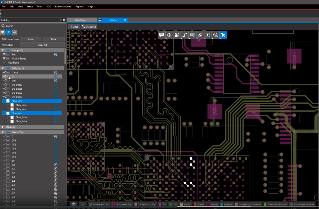
After associating the footprints to the schematic symbols, designers can import the netlist into OrCAD X Presto PCB Editor for design rule setup, placement, and routing. One of the faster methods of tackling the layout is viewing the circuit by functional blocks – essentially, discrete functionality within the greater system. Cross-probing the schematic symbol to see the corresponding footprint (and vice versa) can quickly highlight relevant components for the circuit blocks and allow for easy grouping of near topology during the initial layout placement. Additional design synchronization options in OrCAD X Presto PCB Editor keep the schematic and layout in lock-step for when engineering change orders (ECOs) necessitate addition/removal/modifications of the original schematic.
Procurement and BOM Risk Assessment
The OrCAD X platform further enhances schematic integration with the Live BOM dashboard. Designers can get an immediate evaluation of the risk profile of their board using component information from over 1 billion unique parts. Quickly determine if components are susceptible to ongoing availability issues up to end-of-life/obsolescence from the manufacturer’s announcement. Other concerns like industry compliance (i.e., RoHS) are viewable with a quick filter selection. Engineers can also search for equivalent and drop-in components when available stock or packaging cannot meet the volume of manufacturing lot sizes.

OrCAD X Capture Live BOM provides an up-to-date assessment of BOM risk.
3D Layout and Visibility Controls
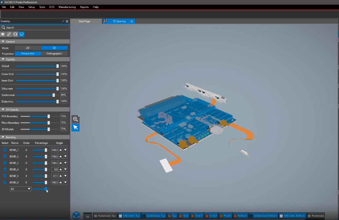
MCAD-ECAD integration for design enclosure has diverse functionality and support with the 3DX Canvas view option. Designers place and route in 3D with the support of a full-bodied 3D design rule check (DRC) that indicates violations of space/overlap constraints in 3D. Alternatively, users can measure air gaps within the 3DX Canvas to confirm that dimensioning between components, enclosure materials, etc., is tolerable. 3D design review benefits from various transparency options, such as opacity and layer toggling for components that can deemphasize individual component visibility.

The 3DX viewer allows users to customize layer opacity for greater visibility during MCAD planning.
Design and Documentation Synchronization
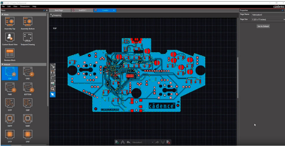
Documentation is straightforward with Live DOC, which automatically synchronizes the board layout to manufacturing outputs. Changes to the layout – like component or silkscreen position – will trigger documentation updates that keep files prepared for packaging and manufacturer review/processing up-to-date. A list of AMSE and ISO page standard sizes is also available, which provides document standardization for the most common manufacturing requirements. Beyond traditional documentation methods, OrCAD X Presto PCB Editor allows users to directly comment within project files with the Design Review and Markup features for even faster team communications.

Live DOC in OrCAD X Presto PCB Editor synchronizes the layout with documentation to prevent errors related to incorrect documentation
Cadence’s Next-Generation Solutions for the Layouts of Tomorrow
Circuit board design software should be robust enough to handle the complexity of modern-day circuit design without being overwhelming or unintuitive. The new OrCAD X Presto PCB Editor is easy to learn and use while offering designers best-in-class functionality and features that synergize with Cadence’s other PCB Design and Analysis Software for an improved ECAD experience. Interested in learning more? See the advantages of the OrCAD X platform first-hand.
Leading electronics providers rely on Cadence products to optimize power, space, and energy needs for a wide variety of market applications. To learn more about our innovative solutions, talk to our team of experts or subscribe to our YouTube channel.