07 - Creating a Schematic
Creating a Schematic
This chapter explains how to create and edit a schematic using either OrCAD Capture or Allegro Design Entry HDL, simulate the schematic using PSpice, and then create and setup a block diagram using MATLAB.
- Creating a Schematic
- Using PSpice to Simulate Schematic
- Creating and Setting up Block Diagram Using MATLAB
Creating a Schematic
You can use either OrCAD Capture or Allegro Design Entry HDL to create and edit schematics.
OrCAD Capture is a schematic design tool set for the Windows environment. With Capture, you can draft schematics and produce connectivity and simulation information for printed circuit boards and programmable logic designs.
Design Entry HDL helps you capture the design of a printed circuit board (PCB) in the schematic form. Design Entry HDL organizes schematic information into pages. It captures and displays only one page of schematic information at a time. Design Entry HDL is a by-reference editor because it references all parts in the schematic from various libraries that reside at the reference or local area. To know more about Design Entry HDL, refer to the Allegro Design Entry HDL User Guide.
Refer to the chapter Designing for other EDA applications of the online OrCAD Capture User Guide on how to incorporate a SPICE netlist into a circuit. Refer to the Transient analysis chapter of the online PSpice User Guide on how to perform transient analysis using PSpice.
The following section explains how to create schematics.
Using OrCAD Capture
Perform the following steps to create a schematic using Capture:
- Create a project in Capture.
- Create the schematic.
To create a new project, perform the following tasks:
- Launch Capture.
- Select File – New – Project.
The New Project dialog box appears. - Specify the project name. In this example, enter MOSCKT in the Name field.
- Specify a work directory in the Location field. For this example, create a directory, Work in the C drive.
- Select Enable PSpice Simulation.
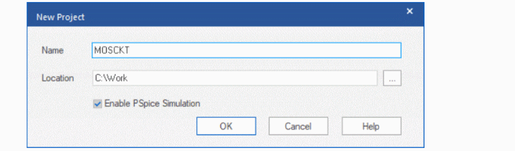
- Click OK.
The Create PSpice Project dialog box appears because you had selected Enable PSpice Simulation check box.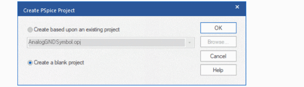
- Select Create a blank project and click OK.
The project window and schematic page is displayed.
You have created the project, now you can create a schematic. Create the circuit as shown in the following figure.
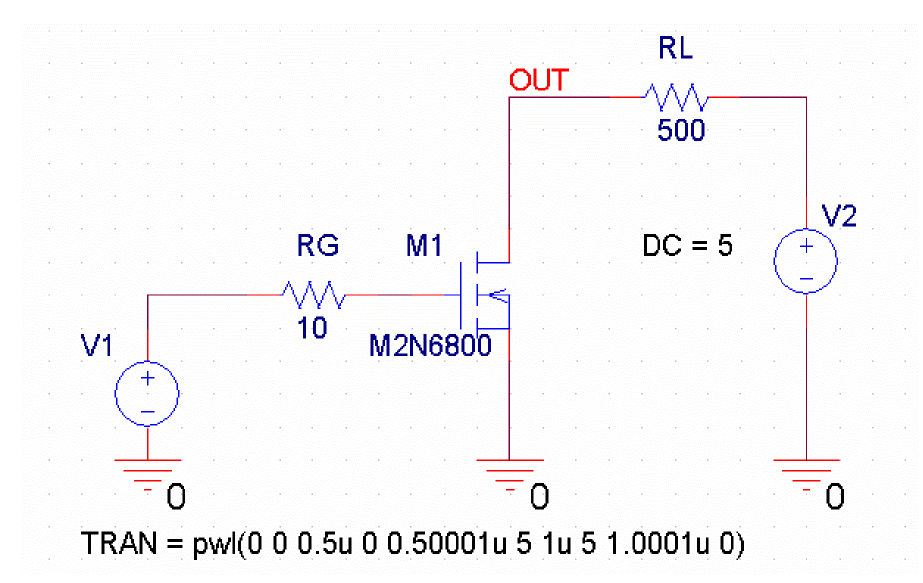
This circuit is comprised of a MOSFET, resistors, and voltage sources. The input signal of the circuit for verifying operation is a 0.5µ wide 1-shot pulse. Attach the node name OUT to the drain node. You will use this name to specify output voltage from the PSpice block later. Use the following libraries to create the schematic design:
|
Library |
Component |
|---|---|
|
pwrmos.olb |
M2N6800 |
|
analog.olb |
R |
|
source.olb |
VSRC |
Select File – Save to save the schematic. You can now use PSpice to simulate the schematic.
Using Design Entry HDL
To create a schematic using Design Entry HDL, perform the following tasks:
- Create a project in Project Manager.
- Create the schematic.
To create a new project:
- Launch Project Manager.
- Select File – New – New Design.
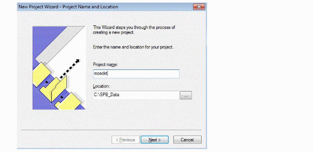
The New Project Wizard appears. You can also click the Create Design Project icon to open the New Project Wizard. - In the Name field, specify the name of the project, mosckt.
In Design Entry HDL, project can contain only lower-case characters, numbers, and the underscore symbol ‘_’.
- In the Location field, specify the path to the directory where you want to create the project.
- Click Next.
The Project Libraries dialog box appears. - Select the required libraries from the list of Available Libraries, and click Add.
The libraries are added to the Project Libraries list. - Click Next.
The Design Name dialog box appears. - In the Design Name field, specify the name of the top-level design.
- Click Next.
The Summary dialog box displays the project details. - Click Finish to create the project.
A message appears to indicate that project creation was successful. - Click OK.
In Project Manager, click the Design Entry icon to open Design Entry HDL. ‘_’.
Using PSpice to Simulate Schematic
PSpice A/D simulates analog-only, mixed analog/digital, and digital-only circuits. PSpice A/D’s analog and digital algorithms are built into the same program so that mixed analog/digital circuits can be simulated with tightly coupled feedback loops between the analog and digital sections without any performance degradation.
Before using PSpice A/D to simulate your design, you need to set up analyses.
PSpice is referred to as PSpice Simulator in Design Entry HDL. As a result, in Design Entry HDL, the PSpice menu is called PSpice Simulator. ‘_’.
To set up analyses, do the following:
- Select PSpice – New Simulation Profile in Capture or PSpice Simulator – New Simulation Profile in Design Entry HDL to open the New Simulation dialog box.
- Specify the name of the simulation profile in the Name field. In this example, specify the name as Tran.
- Select none from the Inherit From list.
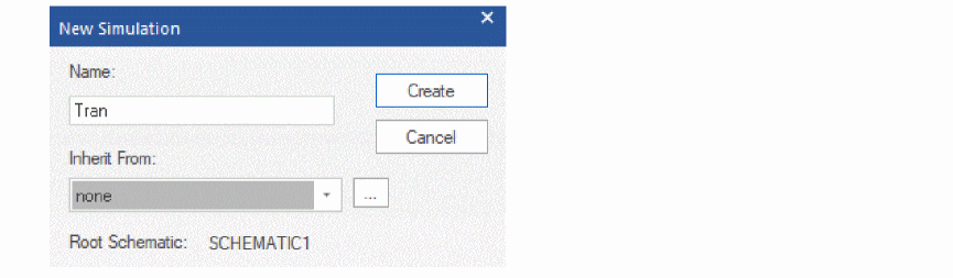
- Click Create. The Simulation Settings dialog box appears. For this example, in the Simulation Settings dialog box:
- Select Time Domain (Transient) as the Analysis Type.
- Specify the Run To Time as 3u (3u seconds).
- Click OK.
You have set up the analyses.
Next, select PSpice – Run to run the simulation. PSpice A/D opens and displays an empty plot window.
Place a marker to display a waveform on the schematic. Select PSpice – Markers – Voltage Level on the MOSFET drain node, as shown in Figure 7-1, to display a drain voltage waveform.
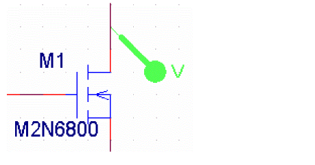
Figure 7-1 Voltage Level on MOSFET
The drain voltage waveform is displayed in the PSpice A/D window, as shown in Figure 7-2.
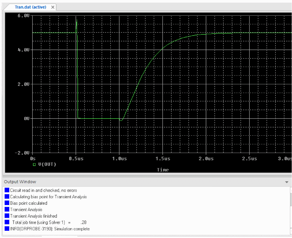
Figure 7-2 Drain Voltage waveform
If a schematic diagram or settings are changed in Capture, you must execute analysis once using PSpice A/D in order for the changes to be reflected in PSpice Simulink Co-simulation. ‘_’.
Creating and Setting up Block Diagram Using MATLAB
In this section, you will learn how to use MATLAB to create a block, set PSpice Simulink Co-simulation block parameters, set up Simulink analyses, and simulate using both PSpice and Simulink.
Creating a Block
To create a block, perform the following tasks:
- Launch MATLAB.
- Using the MATLAB Command Window, set the current MATLAB directory to be the work directory where PSpice files are saved.
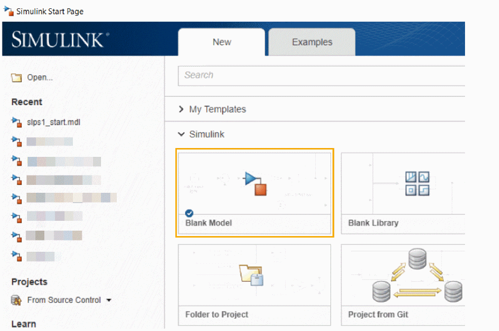
- Under the Home Tab, in the File section, click the New menu and select Simulink Model to create a new model.
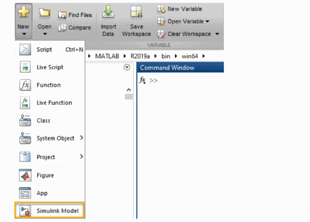 The Simulink Start Page appears.
 - Under the Simulink section, click Blank Model.
 The Simulink model window opens.
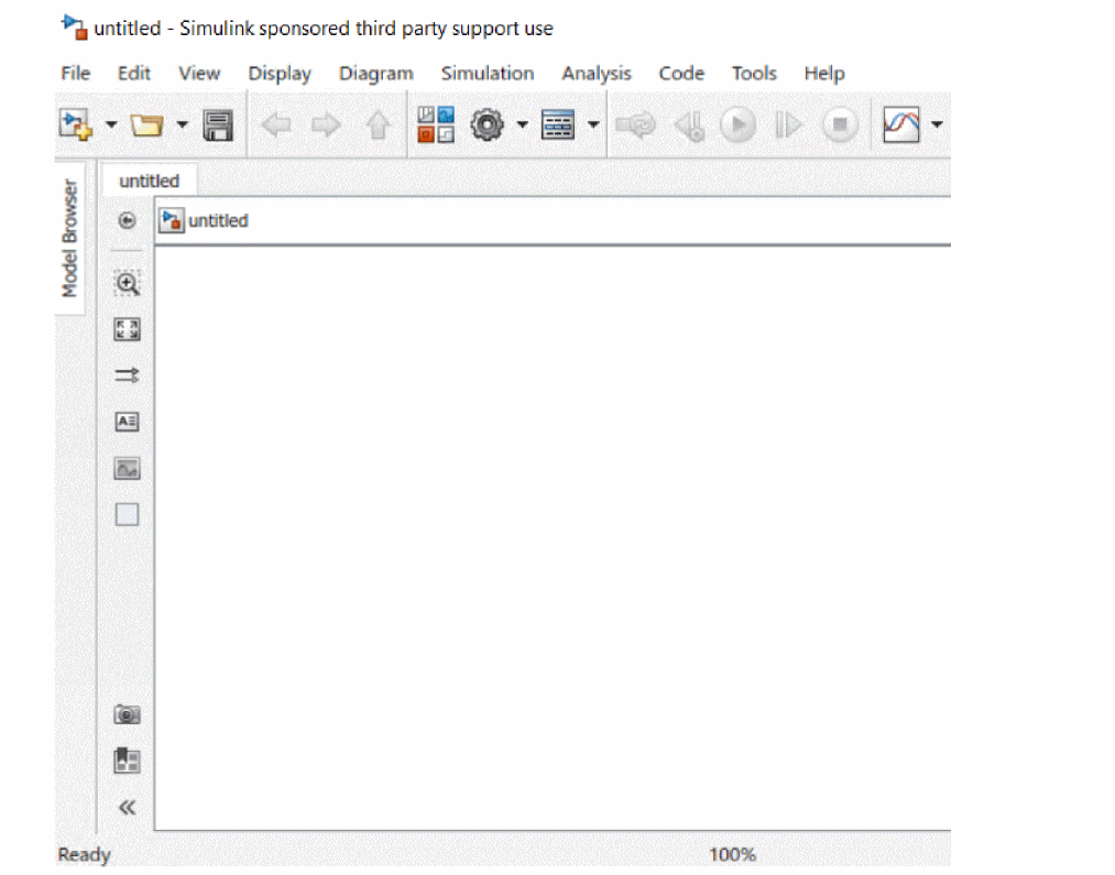
- Click the Library Browser icon or select View – Library Browser.
The Simulink Library Browser window appears.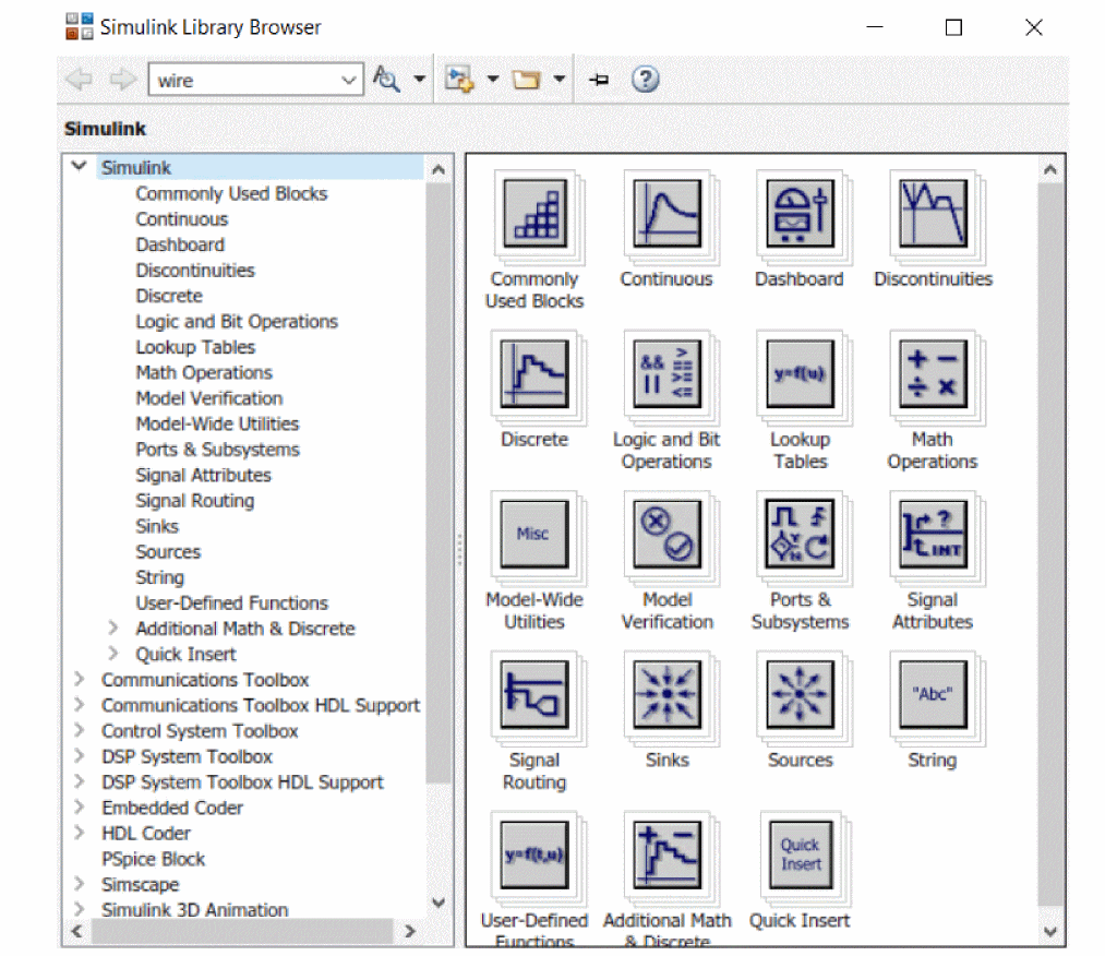
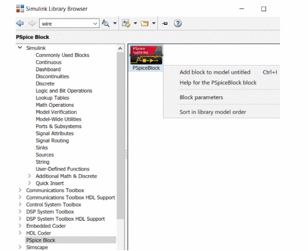
- Select PSpice Block from the left pane.
- Right-click PSpice Block in the right pane and select Add block to model untitled, or drag this icon into the Simulink project window.
- Create a block diagram. In this example, create a block diagram as shown in Figure 7-3, using the blocks, Repeating Sequence/Sources and Scope/Sinks.
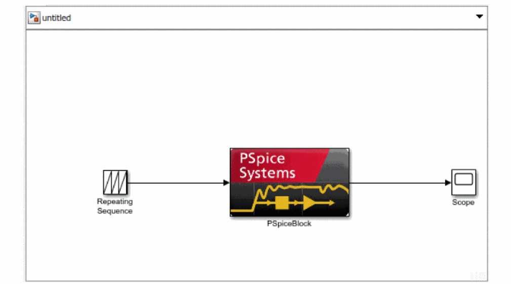 Figure 7-3 Block diagram using Repeating Sequence/Source and Scope/Sinks
 - Double-click the Repeating Sequence block to specify the repeating sequence parameters as shown in Figure 7-4.
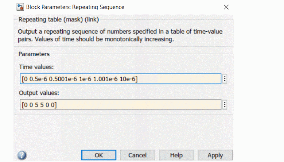 Figure 7-4 Repeating Sequence parameters
 - Click Apply and OK.
The graphic of Repeating Sequence changes.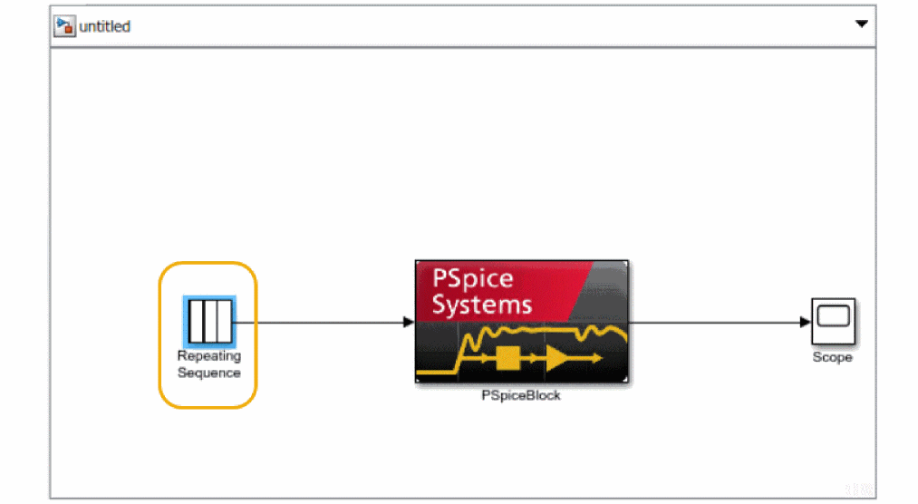
- Select File – Save to save this Simulink model in the current directory. In this example, use the file name as mosckt.slx
You can place only one PSpice Block in a single Simulink model. If you want to incorporate multiple circuits, use Capture to create multiple circuit diagram pages within a project, and connect all the data lines in the Simulink model, which need to be connected to the circuit, to a single PSpice block.
Now that you have created a block and saved it, you will specify the block parameters.
If you have existing PSpice SLPS designs, you need to manually migrate them to the new PSpice Co-simulation format before you can use those designs in new the PSpice Co-simulation environment. For details, see, Migrating Existing PSpice SLPS Designs to New PSpice Simulink Co-simulation Design.
Setting Up PSpice Block Parameters
You need to specify the following main parameters for the PSpice block:
- Capture project file location
- Input sources and outputs for the PSpice block
- PSpice simulation and data collection options
Double-click the PSpice block to open the Co-Simulation Settings window.
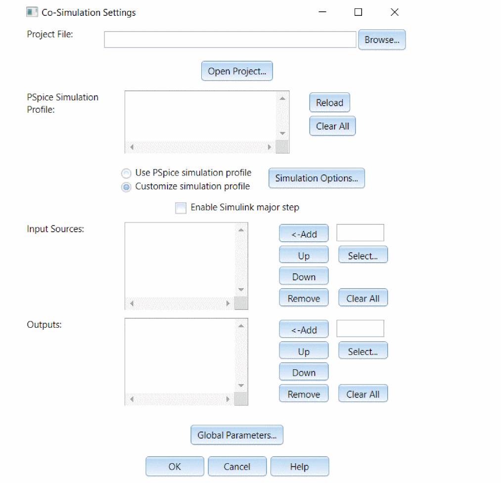
Specify the following parameters:
- Specify the Capture project file path for MOSCKT.opj in Project File field. You can also use the Browse button to specify the project file path.
- Click the Select button under Input Sources.
The Inputs dialog box opens. Select the power source that you want to designate as the source for the PSpice block. In this example, select the source V1.
At least one input must be designated for PSpice Simulink Co-simulation, but you may want to assign a circuit with only output to PSpice Simulink Co-simulation (i.e. an oscillator). In this case, create a dummy circuit (for example, with a power source and resistance) within the circuit diagram page, do not connect it with the original circuit, and allocate some data to this power source.
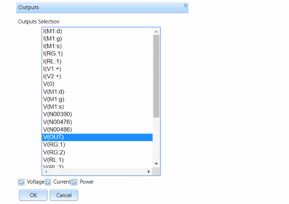
- Click the Select button under Outputs. Specify an output for the PSpice block. In this example, select V(OUT) from the list displayed in the Outputs dialog box.
- After specifying the input sources and output, you can also specify the following:
- Simulation options
- Data collection options
In the Co-simulation Settings window, click the Simulation Options button.
The Simulation Settings window appears.
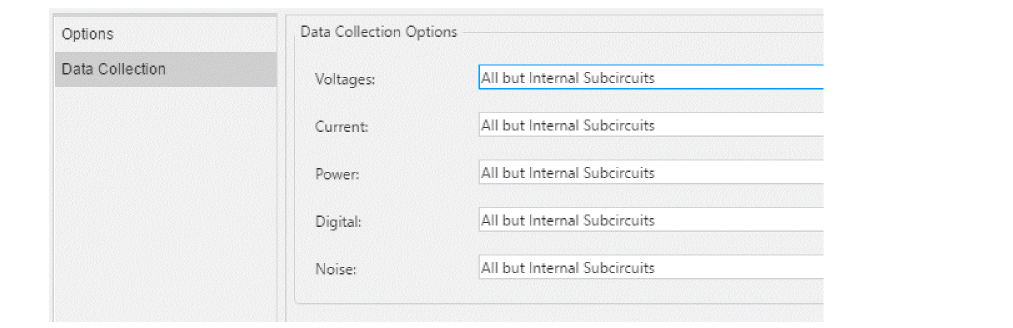
Click the Data Collection tab and select the required option from the drop-down menu. If you select All, more data will be generated and the analysis speed will be slower. Therefore, it is not recommended to change the default value for any of these options unless you need it.
In the Co-simulation Settings window, click the Global Parameters button. The Global Parameters window appears. Specify any already existing global parameters in the Capture design in this dialog box.
After completing the required settings, click OK to close the Co-Simulation Settings window. You can now set up Simulink analyses.
Setting Up Simulink Analyses
You can use the Configuration Parameters dialog box to set up a Simulink analyses.
In the Simulink project window, select Simulation – Model Configuration Parameters. The Configuration Parameters dialog box appears.
For this example, specify the following parameters in the Configuration Parameters dialog box:
- Under Simulation time, specify 3e-6 (3usec) in the Stop time field.
- Under Solver options:
- In the Type list box, select Fixed-step.
- In the Solver list box, select discrete (no continuous states).
- Under Solver details, in the Fixed-step size (fundamental sample time) list box, specify 1e-9.
Figure 7-5 Configuration Parameters dialog box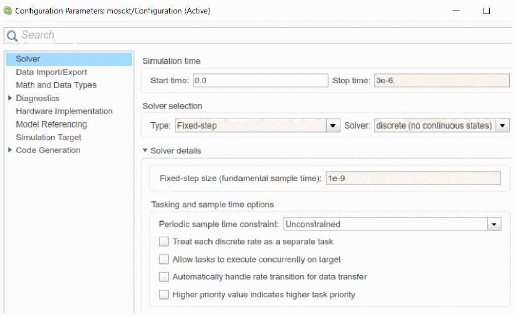
- Click OK.
- In the Simulink project window, select File – Save to save the parameter settings.
- Click OK.
- In the Simulink project window, select File – Save to save the parameter settings.
Simulating and Verifying Results
You can now simulate the analyses using Simulink and then verify the PSpice block results from both Simulink and PSpice.
To simulate using Simulink project window, select Simulation – Run. When analysis is finished, double-click Scope to display the waveform.
The waveform that appears in Simulink, shown in Figure 7-6, is similar to the one displayed PSpice.
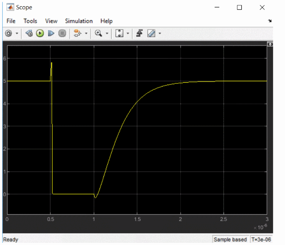
Figure 7-6 The waveform in the Scope window
The simulation results are also available in PSpice.
For this example, to see the PSpice Simulink Co-simulation simulation results in PSpice, perform the following tasks:
- From PSpice, select File – Open.
- Navigate to the location:
<current_project_directory>\MOSCKT-PSpiceFiles\SCHEMATIC1\Tran_slps_\ - Select Tran_slps__SLPS.dat and click Open.
- Select Trace – Add Trace.
The Add Traces dialog box opens. - Select V(X_PSpiceBlock.Out).
- Click OK.
The PSpice Probe window displays the PSpice Simulink Co-simulation simulation result, as shown in Figure 7-7:
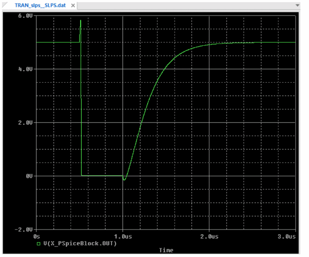
Figure 7-7 PSpice Simulink Co-simulation simulation result in PSpice
Before co-simulation, if select None in the Data Collection tab of the Simulation Settings window, simulation results are not saved in PSpice.
Migrating Existing PSpice SLPS Designs to New PSpice Simulink Co-simulation Design
PSpice Simulink Co-simulation allows you to easily migrate the existing PSpice SLPS designs to new PSpice Simulink Co-simulation designs.
To use the existing designs in the new solution, you need to only replace the existing SLPS block with the new PSpice block. Once done, the existing designs will run in the new solution.
Migrating Single SLPS Block
To replace the old SLPS block in existing designs, do the following:
- Perform the following pre-migration tasks:
- Open the old Simulink design in MATLAB.
- Double-click the old SLPS block.
- Note the old interface settings. These will be used to specify the settings in the new PSpice block.
- Migrate the old Simulink designs to work in the new PSpice Simulink Co-simulation solution. To do so:
- Ensure that:
- You have set up the PSpice Simulink Co-simulation solution. For details, see Setting Up the PSpice Simulink Co-simulation Solution.
- You remove the existing PSpice-SLPS solution path (<installation_directory>\tools\pspice\slps) from the MATLAB’s path settings.
- Open MATLAB from PSpice using Tools – MATLAB – Co-Simulation.
- In the MATLAB Command Window, browse to the directory of the old design.
- In the left panel, double-click the old.mdl/.slx file.
The Simulink project window opens. - Click the Library Browser icon or select View – Library Browser.
The Simulink Library Browser window appears. - Select PSpice Block from Simulink Library Browser.
- Drag and drop the PSpice block to the Simulink project window.
- Replace the old SLPS block with the new PSpice block, placed in the previous step.
- Double click this new block and specify the input and output port connections that you had noted for the old block.
- Save the Simulink design.
- Ensure that:
Migrating Multiple SLPS Blocks
If you have more than one SLPS blocks in your design, perform the following migration tasks:
- Open the design containing multiple SLPS blocks in MATLAB.
- Double click each SLPS block to:
- See the Capture projects they are mapped to
- Note their interface settings. These will be used to specify the new settings in the single new PSpice block.
- For this example, open both the projects in Capture.
- Create a new Capture project and add these two designs to this project.
- Save the project and run simulation.
- Open MATLAB from PSpice using Tools – MATLAB – Co-Simulation.
- In the MATLAB Command Window, browse to the directory that contains the old design with multiple SLPS blocks.
- From the left panel, open this design and modify it to:
- Replace the two old blocks with the new PSpice block.
- Connect the Simulink interfaces mapping of the old blocks to the new block.
- Double click the new PSpice block and specify the new interface settings in the Co-Simulation Settings window.
- Save the design.
- In the Simulink project window, select Simulation – Run.
View the next document: 08 - Interfacing PSpice Designs in MATLAB
If you have any questions or comments about the OrCAD X platform, click on the link below.
Contact Us