17 - Simulating Capture Designs Using PSpice
Overview
PSpice is a simulation program that models the behavior of a circuit. You can use PSpice to test and refine your design before manufacturing the physical board or IC. PSpice supports analyzes that can simulate analog-only, mixed-signal, and digital-only circuits.
Overview of Simulation Using PSpice
To simulate your design in PSpice:
- Ensure that you have PSpice license.
- Create a design using parts that can be simulated.
While creating the designs for simulation, you need to use parts that PSpice can simulate. These parts are available in the PSpice part libraries. You can also associate PSpice models to Capture parts to be able to simulate the parts. A part needs to have an associated model (Implementation type = PSpice Model) and property defined to simulate the part in PSpice. - Create a simulation profile.
After completing the design circuit, you can create a simulation profile using the Simulation Settings dialog box. While creating a simulation profile, specify the types of analysis type and its various parameters, configuration file settings, and so on. - Run PSpice and view results.
When you run PSpice from Capture, a netlist is generated and the PSpice probe window appears. The netlist contains the connectivity information and the analyses type. To view the output of a simulation, you can:- place markers in Capture
- add traces in the PSpice probe window
Creating Design for Simulation
A design that is targeted for simulation has:
- parts for which simulation models are available and configured
- sources of stimulus to the circuit
When creating designs for both simulation and printed circuit board layout, some of the parts you use are for simulation only (simulation stimulus parts like voltage sources), and some of the parts you use have simulation models that only model some of the pins of a real device.
The parts that are to be used for simulation, but not for board layout, have a SIMULATIONONLY property.
You can add this (or any) property to your own custom parts to make them simulation-only.
Adding PSpice and Parametrized Libraries and Parts
The PSpice part libraries (.OLB files) are located in the tools\capture\library\pspice directory, under your main installation directory. The simulation model libraries (.lib files) are located under the tools\pspice\library directory.
If you wish to add more PSpice part libraries to your design, you can do so by using the Place Part dialog box (choose Place – Part or use the Place Part toolbar button). Then add the library you need by selecting it from the tools\capture\library\pspice sub-directory. The PSpice libraries located in the pspice sub-directory include:
- vendor-supplied parts
- passive parts
- breakout parts
- behavioral parts
- special simulation-only parts
 ) appears for a part that can be simulated.
You can also add more PSpice Parts using PSpice Part Search (choose Place - PSpice Component - Search).
At minimum, a part that you can simulate has these properties:
- A simulation model to describe the part's electrical behavior; the model can be:
- explicitly defined in a model library,
- built into PSpice, or
- built into the part (for some kinds of analog behavioral parts).
- A part with modeled pins to form electrical connections on your schematic.
- A translation from the design part to the netlist statement so that PSpice can read it in.
Special simulation-only parts
The PSpice part libraries also include special parts that you can use only for simulation. These include:
- stimulus parts to generate input signals to the circuit (see Defining Stimuli )
- ground parts required by all analog and mixed-signal circuits, which need reference to the ground
- simulation control parts to do things like set bias values
- output control parts for generating tables and line-printer plots to the PSpice output file
Vendor-supplied parts
The PSpice libraries provide an extensive selection of manufacturers' analog and digital parts. Typically, the library name reflects the kind of parts contained in the library and the vendor that provided the models. For example, MOTOR_RF.OLB and MOTOR_RF.LIB contain parts and models, respectively, for Motorola-made RF bipolar transistors.
Two types of libraries are provided with PSpice:
- Standard PSpice libraries
- PSpice Advanced Analysis libraries
Standard PSpice libraries
The standard PSpice libraries are installed in the following locations in the installation directory:
- Capture symbols for standard PSpice libraries at \tools\capture\library\pspice
- Standard PSpice model libraries at \tools\psice\library\
PSpice Advanced Analysis Libraries
The PSpice Advanced Analysis libraries contain over 4,300 analog parts. The Advanced Analysis libraries contain parameterized and standard parts. The majority of the parts are parameterized. The parametrized parts have tolerance, distribution, optimizable and smoke parameters that are required by the PSpice Advanced Analysis tools. Standard parts in the Advanced Analysis libraries are similar to parts in the standard PSpice libraries.
The parametrized parts are associated with template-based PSpice models. An important advantage of using the template-based PSpice models is that you can pass simulation parameters as properties from the schematic editor. For example, if a template-based model is associated with a part, the simulation parameters that you specify on an instance of the part in your design will be passed to the model. There is no need to edit the model itself to change a parameter value. This is unlike the standard PSpice parts that are associated with device characteristic curve-based PSpice models, where you need to edit the model to change a simulation parameter. For more information on template-based and device characteristic curve-based PSpice models, see Chapter 4, "Creating and editing models", in the PSpice User Guide.
Use parametrized parts from Advanced Analysis libraries if you want to analyze the part with an Advanced Analysis tool.
| Advanced Analysis tool | Part Parameters |
|---|---|
| Sensitivity | Tolerance parameters |
| Optimizer | Optimizable parameters |
| Smoke | Smoke parameters |
| Monte Carlo | Tolerance parameters, Distribution parameters (default parameter value is Flat / Uniform) |
The Advanced Analysis libraries are installed in the following locations in the installation directory:
- Capture symbols for Advanced Analysis libraries at
\tools\capture\library\pspice\advanls\
- PSpice Advanced Analysis model libraries at
\tools\pspice\library
The parts in the Advanced Analysis libraries are listed in the online PSpice Advanced Analysis Library List. For information on finding parts using the online PSpice Advanced Analysis Library List, see Finding the part that you want. To find out more about each model library, read the comments in the .lib file header.
Part naming conventions
The part names in the PSpice libraries usually reflect the manufacturers' part names. If multiple vendors supply the same part, each part name includes a suffix that indicates the vendor that supplied the model.
Searching for Parts
To find parts using the part browser, do the following:
- In Capture, choose Place – Part.
-
In the Part Name field, type a text string with wildcard characters that approximates the part name that you want to find. Use this syntax:
<wildcard><part_name_fragment><wildcard>
where <wildcard> is one of the following:* match zero or more characters ? match exactly one character The parts browser displays only the matching part names.
This method finds any part contained in the current part libraries configuration, including parts for user-defined models.
Passive parts
The PSpice libraries supply several basic parts based on the passive device models built into PSpice. These are summarized in the following table.
| Available Parts | Device Type | PSpice Device Letter... |
|---|---|---|
| C C_VAR | capacitor | C |
| L | inductor | L |
| R R_VAR | resistor | R |
| XFRM_LINEAR K_LINEAR | transformer | K and L |
| T | ideal transmission line | T |
| TLOSSY | Lossy transmission line | T |
| TnCOUPLED TnCOUPLEDX* KCOUPLEn* | coupled transmission line | T and K |
*For these device types, the PSpice libraries supply several parts. Refer to the online PSpice Reference Manual for the available parts.
Breakout parts
The PSpice libraries supply passive and semiconductor parts with default model definitions that define a basic set of model parameters. This way, you can easily:
- assign device and lot tolerances to model parameters for Monte Carlo and sensitivity/worst-case analyses
- define temperature coefficients
- define device-specific operating temperatures
These are called breakout parts and are summarized in the following table.
| Breakout Part | Device Type | PSpice Device Letter |
|---|---|---|
| BBREAK | GaAsFET | B |
| CBREAK | capacitor | C |
| DBREAKx | diode | D |
| JBREAKx* | JFET | J |
| KBREAK | inductor coupling | K |
| LBREAK | inductor | L |
| MBREAKx* | MOSFET | M |
| QBREAKx* | bipolar transistor | Q |
| RBREAK | resistor | R |
| SBREAK | voltage-controlled switch | S |
| TBREAK | transmission line | T |
| WBREAK | current-controlled switch | W |
| XFRM_NONLINEAR | transformer | K and L |
| ZBREAKN | IGBT | Z |
* For this device type, the PSpice libraries supply several breakout parts. Refer to the online PSpice Reference Manual for the available parts.
Behavioral parts
Behavioral parts allow you to define how a block of circuitry should work without having to define each discrete component.
Analog behavioral parts
These parts use analog behavioral modeling (ABM) to define each part's behavior as a mathematical expression or lookup table. The PSpice libraries provide ABM parts that operate as math functions, limiters, Chebyshev filters, integrators, differentiators, and others that you can customize for specific expressions and lookup tables. You can also create your own ABM parts.
Digital behavioral parts
These parts use special behavioral primitives to define each part's functional and timing behavior. These primitives are:
| LOGICEXP | to define logic expressions |
| PINDLY | to define pin-to-pin delays |
| CONSTRAINT | to define constraint checks |
Many of the digital parts provided in the PSpice libraries are modeled using these primitives. You can also create your own digital behavioral parts using these primitives.
Defining Part Properties Needed for Simulation
If you want to use a part for simulation, then your part should have the PSPICETEMPLATE property defined for it:
You can also add other simulation-specific properties for digital parts: IO_LEVEL, MNTYMXDLY, and PSPICEDEFAULTNET.
Here are the things to check when editing part properties:
- Does the property specify the correct number of pins/ nodes?
- Are the pins/ nodes in the specified property in the proper order?
- Do the pin/ node names in the property match the pin names on the part?
For examples of how to use the property, see PSPICETEMPLATE examples.
Editing simulation properties
To edit a property needed for simulation, do the following:
- In the schematic page editor, select the part to edit.
- From the Edit menu, choose Properties to display the Parts spreadsheet of the Property Editor.
- Click on the cell of the column you want to change, or click the New button to add a property (and type the property name in the Name field).
- If needed, type a value in the Value text box.
- Click Apply to update the design, then close the spreadsheet.
PSPICETEMPLATE property
The PSPICETEMPLATE property defines the PSpice syntax for the part's netlist entry. When creating a netlist, Capture substitutes actual values from the circuit into the appropriate places in the PSPICETEMPLATE syntax, then saves the translated statement to the netlist file.
Any part that you want to simulate must have a defined PSPICETEMPLATE property. These rules apply:
- The pin names specified in the PSPICETEMPLATE property must match the pin names on the part.
- The number and order of the pins listed in the PSPICETEMPLATE property must match those for the associated .MODEL or .SUBCKT definition referenced for simulation.
- The first character in a PSPICETEMPLATE must be a PSpice device letter appropriate for the part (such as Q for a bipolar transistor).
PSPICETEMPLATE syntax
The PSPICETEMPLATE contains:
- regular characters that the schematic page editor interprets verbatim, and
- property names and control characters that the schematic page editor translates.
Regular characters in template
Regular characters include the following:
- alphanumeric
- any keyboard part except the special syntactical parts used with attributes (@ & ? ~ #)
- whitespace
An identifier is a collection of regular characters of the form:
alphabetic character [any other regular character]*.
Property names in templates
Property names are preceded by a special character as follows:
[ @ | ? | ~ | # | & ]<identifier>
The schematic page editor processes the property according to the special character as shown in the following table.
| Syntax* | Replacement |
|---|---|
| @<id> | Value of <id>. Error if no <id> property or if no value assigned. |
| &<id> | Value of <id>, if <id> is defined. |
| ?<id>s...s | Text between s...s separators, if <id> is defined. |
| ?<id>s...ss...s | Text between the first s...s separators, if <id> is defined, else the second s...s clause. |
| ~<id>s...s | Text between s...s separators, if <id> is undefined. |
| ~<id> s...ss...s | Text between the first s...s separators, if <id> is undefined, else the second s...s clause. |
| #<id>s...s | Text between s...s separators, if <id> is defined, but delete rest of template if <id> is undefined. |
*s is a separator character.
Separator characters include commas (,), periods (.), semi-colons (;), forward slashes (/), and vertical bars ( | ). You must always use the same character to specify an opening-closing pair of separators.
The caret (^) character in templates
The schematic page editor replaces the caret (^) character with the complete hierarchical path to the device being netlisted.
The new line (\n) character sequence in templates
The part editor replaces the new line (\n) character sequence with a new line. Using newline character sequence (\n), you can specify a multiline netlist entry from a one-line template.
The percentage (%) character and pin names in templates
Pin names are denoted as follows:
%<pin name>
where pin name is one or more regular characters.
The schematic page editor replaces the %<pin name> clause in the template with the name of the net connected to that pin.
The end of the pin name is marked with a separator.
Net Name Translation
To avoid name conflicts in PSpice, the schematic page editor translates the following characters contained in pin names.
| Pin name character | Replacement |
|---|---|
| < | LT |
| > | GT |
| = | EQ |
| \XXX\ | XXXbar |
Templates for devices in the part library start with a PSpice device letter, followed by the hierarchical path, and then the reference designator (REFDES) property. We recommend that you adopt this scheme when defining your own netlist templates.
PSPICETEMPLATE examples
Simple resistor (R) template
The R part has two pins (1 and 2) and two required properties, REFDES and VALUE.
The template for the resistor is:
R^@REFDES %1 %2 @VALUE
A sample translation of the template is:
R_R23 abc def 1k
where REFDES equals R23, VALUE equals 1k, and R is connected to nets abc and def.
Voltage source with optional AC and DC specifications (VAC) template
The VAC part has two properties, AC and DC, and two pins, + and -.
The template is:
V^@REFDES %+ %- ?DC|DC=@DC| ?AC|AC=@AC|
A sample translation of the template is:
V_V6 vp vm DC=5v
where REFDES equals V6, VSRC is connected to nodes vp and vm, DC is set to 5v, and AC is undefined.
Another sample translation of the template is:
V_V6 vp vm DC=5v AC=1v
where, in addition to the settings for the previous translation, AC is set to 1v.
Parameterized subcircuit call (X) template
This example supposes a subcircuit Z that has two pins (a and b) and a subcircuit parameter G, where G defaults to 1000 when no value is supplied.
To allow the parameter to be changed on the schematic page, treat G as property in the template.
The template is:
X^@REFDES %a %b Z PARAMS: ?G|G=@G|
~G|G=1000|
An equivalent template (using the if...else form) is:
X^@REFDES %a %b Z PARAMS: ?G|G=@G||G=1000|
A sample translation of the template is:
X_U33 101 102 Z PARAMS: G=1024
where REFDES equals U33, G is set to 1024, and the subcircuit connects to nets 101 and 102.
Another sample translation of the template is:
X_U33 101 102 Z PARAMS: G=1000
where the settings of the previous translation apply except that G is undefined.
Digital stimulus parts with variable width pins template
For a digital stimulus device template (such as that for a DIGSTIM part), a pin name can be preceded by an asterisk (*) character. This signifies that the pin can be connected to a bus and the width of the pin is set to be equal to the width of the bus.
The template is:
U^@REFDES STIM(%#PIN, 0) %*PIN
\n+ STIMULUS=@STIMULUS
where #PIN refers to a variable width pin.
A sample translation of the template is:
U_U1 STIM(4,0) 5PIN1 %PIN2 %PIN3 %PIN4
+ STIMULUS=mystim
where the stimulus is connected to a four-input bus, a[0-3].
Pin callout in subcircuit templates
The number and sequence of pins named in a template for a subcircuit must agree with the definition of the subcircuit itself--that is, the node names listed in the .SUBCKT statement, which heads the definition of a subcircuit. These are the pinouts of the subcircuit.
IO_LEVEL property
The IO_LEVEL property defines the level of interface subcircuit model PSpice must use for a digital part that is connected to an analog part.
If you are creating a digital part, you need to
-
Add the IO_LEVEL property to the part and assign a value shown in the table below.
Value Interface subcircuit (level) 0 circuit-wide default 1 AtoD1 and DtoA1 2 AtoD2 and DtoA2 3 AtoD3 and DtoA3 4 AtoD4 and DtoA4 - Use this property in the property definition (IO_LEVEL is also a subcircuit parameter used in calls for digital subcircuits).
MNTYMXDLY property
The MNTYMXDLY property defines the digital propagation delay level that PSpice must use for a digital part.
If you are creating a digital part, you need to do the following
-
Add the MNTYMXDLY property to the part and assign a value shown in the table below.
Value Propagation delay 0 circuit-wide default 1 minimum 2 typical 3 maximum 4 worst-case (min/max) - Use this property in the property definition (MNTYMXDLY is also a subcircuit parameter used in calls for digital subcircuits).
PSPICEDEFAULTNET property
The PSPICEDEFAULTNET pin property defines the net name to which a power or ground (invisible) pin is connected.
For example, if the power and ground pins on a digital part are connected to the digital nets $G_DPWR and $G_DGND, respectively, then the properties are defined as follows:
PSPICEDEFAULTNET=$G_DPWR
PSPICEDEFAULTNET=$G_DGND
If you are creating a digital part, you need to do the following
- For each power pin, create a PSPICEDEFAULTNET property and assign the name of the digital net to which the pin is connected.
- Use the appropriate pin name in the property definition.
Guidelines and Best Practices for Specifying Values for Part Properties
Note the following when specifying values for part properties:
- Do not leave a space between the value and its unit, if the unit is a scale symbol. For example, specify 5K instead of 5 K.
- You can use the European notation, where the decimal point is omitted and replaced by the unit symbol, for specifying values. For example, you can use 3K3, which is the European notation for 3.3K.
- Specify tolerance values as percentages. If you specify an absolute value, the tolerance value will be read as an absolute number. For example, if you specify the value of the POSTOL property as a percentage, say 10%, on a 10K resistor, the distribution values will be taken in the range of 10K?1K. If you specify the tolerance value as an absolute number, say 10, the distribution values will be taken in the range of 10K?10?
- Do not add any space for the name of an hierarchical block.
Placing PSpice Ground 0 Symbols for PSpice Simulations
For PSpice analog simulation to run, your design must have a PSpice ground (0) symbol. The CAPSYM.OLB, which is the default library in Capture, includes the PSpice ground (0) symbol. Use the 0 symbol to place a PSpice ground 0 symbol in your design.
To select the 0 symbol, do the following:
- Choose Place – Ground (or use the Place Ground toolbar button). The Place Ground dialog box appears.
-
Select the CAPSYM part library from the Libraries list (if it is not already selected).
You can also place the 0 symbol from the Source part library. To do this, add the Source part library to the Libraries list using the Add Library button; SOURCE.OLB is located in the \TOOLS\CAPTURE\LIBRARY\PSPICE subdirectory under your installation directory. - Select the 0 symbol (if not already selected).
-
Click OK to place the PSpice ground 0 symbol.
Alternatively:
- You can place any ground symbol, open the Property Editor, and change its name to 0.
- You can place PSpice ground 0 symbol from PSpice Component quick pick, that is, Place - PSpice Component - PSpice Ground.
Using the FLOAT Property for Unconnected Pins
When preparing a circuit for simulation with PSpice, it is important that all pins for all parts are connected properly. If a pin is meant to remain unconnected intentionally, you need to use the PSpice pin property FLOAT, rather than a No Connect symbol. Otherwise, the circuit may not netlist correctly for PSpice.
The pin property FLOAT may have one of the following three values:
| Value | Description |
|---|---|
| Error | The pin will not netlist. An error message will be returned when the PSpice simulation netlist is generated. Use Error when you want to be reminded that this pin is a "no connect" and should be treated in a special way. Error is the default value. |
| RtoGND | The pin is connected to a virtual resistor, whose opposite pin is tied to GND. The resistor has a value of 1/GMIN. This value allows the simulation netlist to be created and allows PSpice to perform the analysis. The virtual resistor will not be processed as part of a layout netlist or appear in a BOM. |
| UniqueNet | The pin, when left unconnected, is attached to a unique node when the PSpice simulation netlist is generated. Use UniqueNet when you want the pin to remain unconnected but correspond to the Probe data associated with its part. |
The FLOAT property can either be defined in the part editor when creating a new part, or you can edit a pin on an existing part using the property editor.
To define the FLOAT property using the property editor
- In Capture, double-click on the pin to open the property editor spreadsheet.
- Click on the Pins tab.
- Click New Property and type FLOAT (upper case) in the Name text box.
- Type the property value you want to use, then click OK.
- Click Apply or close the spreadsheet to have the changes take effect.
Using Global Parameters and Expressions
In addition to literal values, you can use global parameters and expressions to represent numeric values in your circuit design.
Global parameters
A global parameter is like a programming variable that represents a numeric value by name.
Once you have defined a parameter (declared its name and given it a value), you can use it to represent circuit values anywhere in the schematic; this applies to any hierarchical level.
Some ways that you can use parameters are as follows:
- Apply the same value to multiple part instances.
- Set up an analysis that sweeps a variable through a range of values (for example, the DC sweep or parametric analysis).
When multiple parts are set to the same value, global parameters provide a convenient way to change all their values for "what-if" analyses.
For example, if two independent sources have a value defined by the parameter VSUPPLY, then you can change both sources to 10 volts by assigning the value once to VSUPPLY.
Declaring and using a global parameter
To use a global parameter in your design, you need to:
- define the parameter using a PARAM part from SPECIAL.OLB.
- use the parameter in place of a literal value somewhere in your design.
To declare a global parameter
- Place a PARAM part in your design.
- Double-click the PARAM part to display the Parts spreadsheet.
- Do the following for each global parameter:
- Click New, then enter NAMEn in the Property Name field, then click OK. This creates a new property for the PARAM part, NAMEn in the spreadsheet.
- Click on the cell below the NAMEn column and enter a default value for the parameter.
-
While this cell is still selected, click Display. In the Display format frame, select Name and Value, then click OK.
System variables have reserved parameter names. Do not use these parameter names when defining your own parameters. - Click Apply to update all the changes to the PARAM part, and then close the spreadsheet.
For example, to declare the global parameter VSUPPLY that will set the value of an independent voltage source to 14 volts, place the PARAM part, and then create a new property named VSUPPLY with a value of 14V.
To use the global parameter in your circuit
- Find the numeric value that you want to replace: a component, model parameter, or other property value.
-
Replace the value with the name of the global parameter using the following syntax:
{ global_parameter_name }
The curly braces tell PSpice to evaluate the parameter and use its value.To avoid errors, always include parameter variable name in curly braces when it is assigned to the parameter/property on the part.
Expressions
PSpice evaluates the expression to a single value every time:
- it reads in a new circuit
- a parameter value used within an expression changes during an analysis.
An example of this would be a parameter that changes with each step of a DC sweep or parametric analysis.
Specifying expressions
To use an expression in your circuit
- Find the numeric or boolean value you want to replace: a component value, model parameter value, other property value, or logic in an IF function test.
- Replace the value with an expression using the following syntax:
{ expression }
where {expression} can contain any of the following:- standard operators (listed in the table below)
- built-in functions (listed in the PSpice User Guide)
- user-defined functions
- system variables (listed in the PSpice User Guide)
- user-defined global parameters
- literal operands
The curly braces tell PSpice to evaluate the expression and use its value.
| Operator class | Operator | Operation |
|---|---|---|
| arithmetic | ||
| + | addition or string concatenation | |
| - | subtraction | |
| * | multiplication | |
| / | division | |
| ** | exponentiation | |
| logical | ||
| ~ | unary NOT | |
| | | boolean OR | |
| ^ | boolean XOR | |
| & | boolean AND | |
| relational* | ||
| == | equality test | |
| != | non-equality test | |
| > | greater than test | |
| >= | greater than or equal to test | |
| < | less than test | |
| <= | less than or equal to test |
*Logical and relational operators are used within the IF() function; for digital parts, logical operators are used in Boolean expressions.
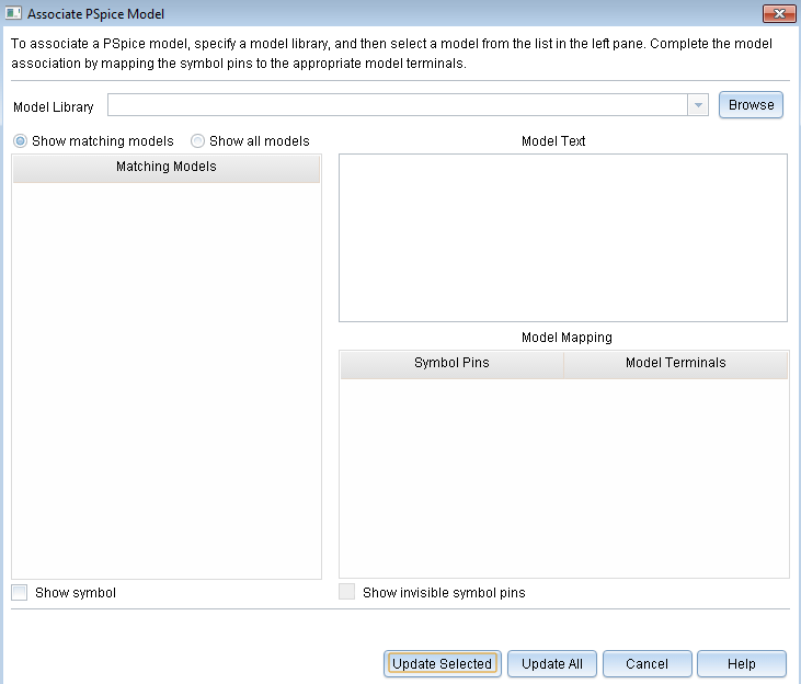
Associating PSpice Model to Capture Parts
You can associate a PSpice model to an existing or new part created in Capture. Before associating a PSpice model to a part, ensure the following:
-
Use this feature on a part placed on the root schematic. If the design is not a root schematic, open the project manager, right-click this schematic, and select Make Root to convert it into a root schematic design.
- Only a single part should be selected at a time.
- PSpice models can only be associated with homogeneous parts.
- If the PSpice model is to be associated to a part in an externally referenced design, you need to open this design separately. Next, associate a PSpice model to the required part, save the design and then reuse it in the root schematic.
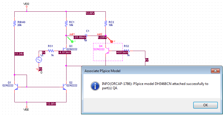
To associate a PSpice model to a Capture part in the schematic editor:
-
Select the Capture part to which you want to associate a PSpice model.
-
Select Tools – Associate PSpice Model.
or
Right-click the part and choose Associate PSpice Model. -
A message appears prompting you to save the design before model association. If the selected part already has an associated model, a message appears to confirm if you want to overwrite this implementation. Click Yes.
The Associate PSpice Model dialog box appears.
 If the symbol is open in Capture, the Associate PSpice Model option will appear disabled in the pop-up menu.
 - Click Browse to specify the name and location of the library containing the required PSpice model. You can either select the library from the Model Library drop-down list box or browse to the library location.
- Once you have selected the
.libfile, the Associate PSpice Model window lists the matching models. By default, the Show matching models option is selected. To view all the models, select the Show all models option.
- Select the required model from the Matching Models section.
-
Map each symbol pin to the correct model terminal in the Model Mapping section. The model terminals for the selected symbol pins appear in the Model Terminals drop-down list.
For mapping, you can view the model definition. When you select a model in the Matching Models section, its definition appears in the Model Text section.
Click the Show symbol check box to preview the symbol along with its sections. The symbol preview can only be seen when the library path specified in Design Cache exists.
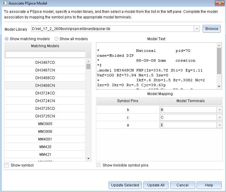
-
Select the Show invisible symbol pins check box to view and map any invisible power pins in the symbol. This check box will appear disabled if there are no such pins.
-
Click Update Selected to complete attaching the selected PSpice model to the selected Capture part and to close the Associate PSpice Model window. A message appears to indicate that the selected model is now attached to the part selected on the schematic editor.
 Update All
If you click Update All, all part instances of the same source package are associated with the selected PSpice model. if you click Update All, and the selected part is also in an externally referenced design, the PSpice model will not be associated to such a part.
-
Click OK.
This automatically saves the design.
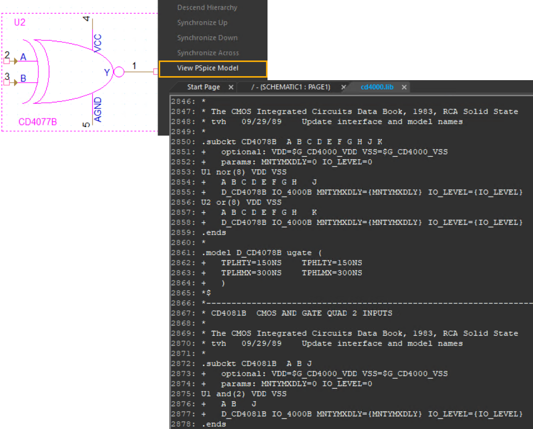
Viewing PSpice Models
This feature allows you for a dedicated and within-Capture view of the PSpice model. For a part placed on the schematic, you can view the information of its associated PSpice model in a separate tab in the canvas area. To do so, right-click a part and select View PSpice Model from the pop-up menu.
This information is read-only. Some of the information may be non-readable if the associated model is encrypted.

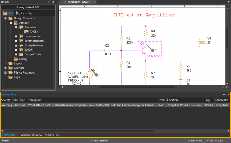
Viewing Information on Missing PSpice Models in Online DRC
For a part placed on the schematic, if the PSpice model associated with the part is not found in the configured libraries, then information related to such a part instance appears as a message in the Online DRC tab of the Output pane.
Importing PSpice Schematic Projects in Capture
You can import a MicroSim Schematics project to a Capture project.
To convert a Schematics project to Capture:
- In Capture, choose File – Import – PSpice.
The Import Design dialog box opens.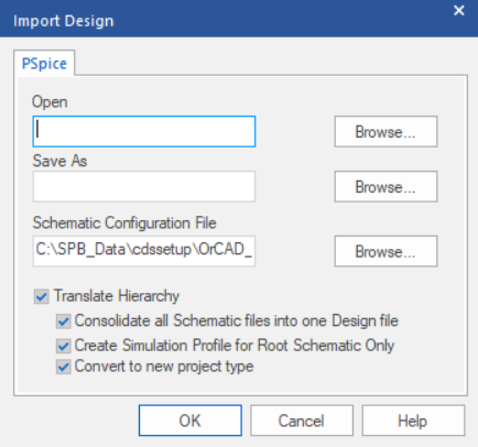
- In the PSpice tab, select the source schematic (Open), the destination project, (Save As) and the PSPICE.INI (Schematic Configuration File) file for existing settings.
-
Click OK to start the automated translation utility.
For detailed information about using the Schematics-to-Capture Translator, see the user guide, Translating Designs from PSpice Schematics to Capture.
Defining Stimuli
To simulate your circuit, you need to connect one or more source parts that describe the input signal that the circuit must respond to .
The PSpice libraries supply several source parts that are described in the tables that follow. These parts depend on:
- the kind of analysis you are running,
- whether you are connecting to the analog or digital portion of your circuit, and
- how you want to define the stimulus: using the Stimulus Editor, using a file specification, or by defining part property values.
Analog stimuli
Analog stimuli include both voltage and current sources. The following table shows the part names for voltage sources.
| Input | Part for voltage |
|---|---|
| DC bias | VDC or VSRC |
| AC magnitude and phase | VAC or VSRC |
| exponential | VEXP or VSTIM |
| periodic pulse | VPULSE or VSTIM |
| piecewise-linear | VPWL or VSTIM |
| piecewise-linear that repeats forever | VPWL_RE_FOREVER or VPWL_F_RE_FOREVER |
| piecewise-linear that repeats n times | VPWL_N_TIMES or VPWL_F_N_TIMES* |
| frequency-modulated sine wave | VSFFM or VSTIM |
| sine wave | VSIN or VSTIM |
*VPWL_F_RE_FOREVER and VPWL_F_N_TIMES are file-based parts; the stimulus specification is saved in a file and adheres to the PSpice netlist syntax.
To determine the part name for an equivalent current source, in the table of voltage source parts, replace the first V in the part name with I. For example, the current source equivalent to VDC is IDC, to VAC is IAC, to VEXP is IEXP, and so on.
Using VSTIM and ISTIM
You can use VSTIM and ISTIM parts to define any kind of time-based input signals. To specify the input signal itself, you need to use the Stimulus Editor.
If you want to specify multiple stimulus types
If you want to run more than one analysis type, including a transient analysis, then you need to use either of the following:
- time-based stimulus parts with AC and DC properties
- VSRC or ISRC parts
Using time-based stimulus parts with AC and DC properties
The time-based stimulus parts that you can use to define a transient, DC, and/or AC input signal are listed below.
| VEXP | IEXP |
| VPULSE | IPULSE |
| VPWL | IPWL |
| VPWL_F_RE_FOREVER | IPWL_F_RE_FOREVER |
| VPWL_F_N_TIMES | IPWL_F_N_TIMES |
| VPWL_RE_FOREVER | IPWL_RE_FOREVER |
| VPWL_RE_N_TIMES | IPWL_RE_N_TIMES |
| VSFFM | ISFFM |
| VSIN | ISIN |
In addition to the transient properties, each of these parts also has a DC and AC property. When you use one of these parts, you must define all of the transient properties. However, it is common to leave DC and/or AC undefined (blank). When you give them a value, the syntax you need to use is as follows.
| Property | Syntax |
|---|---|
| DC | DC_value[units] |
| AC | magnitude_value[units] [phase_value] |
Using VSRC or ISRC parts
The VSRC and ISRC parts have one property for each analysis type: DC, AC, and TRAN. You can set any or all of them using PSpice netlist syntax. When you give them a value, the syntax you need to use is as follows.
| Property | Syntax |
|---|---|
| DC | DC_value[units] |
| AC | magnitude_value[units] [phase_value] |
| TRAN | time-based_type (parameters) |
where time-based_type is EXP, PULSE, PWL, SFFM, or SIN, and the parameters depend on the time-based_type.
Digital stimuli
| Input | Part |
|---|---|
| For transient analyses | |
| DIGSTIMn | signal or bus (any width) |
| DIGCLOCK | clock signal |
| STIM1 | 1-bit signal |
| STIM4 | 4-bit bus |
| STIM8 | 8-bit bus |
| STIM16 | 16-bit bus |
| FILESTIMn | file-based signal or bus (any width) |
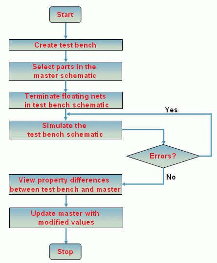
Using Partial Design Simulation
Using the Partial Design Simulation feature, you can:
- Identify individual components of any design and simulate only selected portions
- Simulate different circuits in the design with different simulation profiles
- Create netlist of only a particular portion of the design
- Compare and merge portions of a design quickly
To use this feature, you select a portion called test bench of a master design. You create one or more test benches using the Tools – Test Bench – Create Test Bench menu of OrCAD X Capture. The test benches are listed in the Project Manager window of the master design. You can add components from the design to a test bench by selecting them from the master schematic canvas, and then add profiles and simulate the test bench. You can also synchronize the master design with a test bench, to propagate any changes you make in the test bench design.
You can use the Partial Design Simulation in the following flow, as shown in the figure:
- Create a test bench.
- Select parts in the master schematic.
- Terminate floating nets in test bench schematic.
- Simulate the test bench schematic.
- View Property differences between test bench and master.
- Update the master with modified values.
Working with a Test Bench
A test bench is like any other new project created in Capture. When you create a test bench, it is listed under the TestBenches node in the project manager of the master project. All simulation profiles and parameters or variables in the master project are copied by default to the test bench project. The components in the different schematics are grayed out. You can choose to activate the components to create a partial design.
You might need to add terminations and other parts to the partial design of the test bench because a test bench design must be complete in itself. You can also make edits to your test bench to prepare it for simulation by adding a stimulus or simulation profiles. You can simulate a test bench even if the master design is not a PSpice project. If the master project is a PSpice project, the test bench can inherit the simulation profiles in the master project.
Creating a Test Bench
- Select the DSN file in the Project Manager
- Choose Tools – Test Bench – Create Test Bench
The Test Bench field appears. - Enter a name in the Enter Test Bench Name field.
You can set a default test bench name by adding the Default Test Bench Name property in the [TEST BENCH]section ofcapture.ini. For example, to set the default test bench name toMyTestBench, add the following section incapture.ini:[TEST BENCH]Default Test Bench Name=MyTestBench -
Click OK.
The test bench is added under TestBenches in the Project Manager. The created test bench contains all the designs in the master project.
The components in the schematic pages of the test bench are grayed out. You need to add components to the test bench to be able to work on a partial design.You can activate a test bench by right-clicking on the test bench in the Project Manager under Test Benches and choosing Make Active.
Activating Components
You can activate components in a test bench by using any one of the options; context-menu for selected parts in the master design, conext-menu for selected parts in the test bench design, or from the hierarchy editor.
To activate components from the master design:
- Select the components in the master design.
- Right-click and choose TestBench – Add Part(s) to Active TestBench.
To activate components from the test bench design:
Select the components in the test bench design.
Right-click and choose TestBench – Add Part(s) to Self .
To activate components using the hierarchy editor, check the components to be added in the hierarchy editor of the master design, as shown in the figure.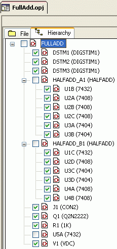
Similarly, you can inactivate a component from the test bench design from the context-menu or the hierarchy editor. Capture will ignore all components that are inactive. As a result, these inactive components will not be processed, for example, for simulation.
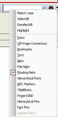
When you activate only a portion of the design, many nets might be floating because they are not terminated. You can easily resolve this problem by making a floating net search. To perform this search: - Select the test bench design in Capture
- From the search menu, select Floating Nets as shown in the figure
- Click the Find button.
All the floating nets requiring terminators are listed in the Floating Nets tab of the Find Window.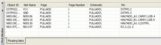
- Double-click a row in the Find Window to select it in the design.
Comparing and Updating Master Design
You can compare the schematics in the master project and the test bench to highlight the differences using the SVS utility. This utility displays the differences and uses color code to highlight the different types of changes. The result window has two panels, the left panel represents the test bench. The differences listed are for the categories: unmatched object (yellow by default), missing objects (red by default), and matching objects (white in color). You can check any of the listed differences on the test bench panel, and propagate the changes to the master design. However, you cannot update a master design for missing objects.
You can click Settings (  ) to open the Settings dialog box and change the default colors in the Color tab. You can also filter for different objects, if you do not want them to be listed.
To compare and propagate changes:
- Select the master DSN in Project Manager.
- Choose Tools – Test Bench – Compare Test Bench.
The differences between the master design and the test bench design are displayed.
To update the master design with the test bench differences, check the differences you want to update in the SVS tab and click Accept Left ( ).
).
Running a Simulation and Viewing Results Using PSpice
This topic discusses how to use PSpice from Capture to create a simulation profile, run a simulation, and view the simulation results in the PSpice Probe window.
Creating New Simulation Profile
A simulation profile (*.SIM) saves your simulation settings for an analysis type so you can reuse them easily. You can create a new simulation profile from scratch or import the settings from an existing simulation profile. Importing settings from existing simulation profiles allows you to reuse the settings from other simulation profiles.
Capture allows you to create a new simulation profile by importing settings from a simulation profile that exists in the same project or in another project.
To create a new simulation profile, do the following:
- Choose PSpice - New Simulation Profile.
The New Simulation dialog box appears. - In the Profile Name text box, type a name for the profile (such as the name of the analysis type for the new profile).
-
You may want to import the simulation settings from an existing profile to the new profile.
-
To select a profile from the current project, click the Inherit From drop-down list. This list shows all the simulation profiles in the current project.
-
To select a profile from another project, click the browse button to navigate to the desired simulation profile.
-
- Click Create to create the profile and display the Simulation Settings dialog box.
The Simulation Settings dialog box appears. -
In the Analysis tab, specify the analysis type.
Specify the relevant settings in the General and other tabs.Check whether you have the nom.lib added as a GLOBAL library under the Library category of the Configuration Files tab. This "master library" file calls out the other libraries that Cadence supplies along with the installation. It takes time for PSpice to scan each library file. PSpice creates an index file, called <filename>.IND, to speed up the search process. The index file is re-created whenever PSpice senses that it might be invalid.
If this nom.lib is not there then Capture-PSpice interface will not be able to detect the Cadence-supplied PSpice libraries to be used in the simulation, so add this globally. The nom.lib resides in the <install dir>/tools/pspice/library folder.
- Click OK to save the settings and close the dialog box.
After creating a new profile, you can edit the settings with the PSpice – Edit Simulation Settings command.
Shortcut
Keyboard: ALT+S+N
Imported Parts in Schematic Design
The PSpice for TI installation comes with a set of pre-installed libraries. A design can include parts or models from these pre-installed libraries as well as imported parts from external libraries.
When parts with imported models are used in a design, a corresponding message is displayed in the Online DRCs window.

When you run a PSpice simulation on a design containing imported models, you can place at least one and, at the most, four markers for data collection. Any marker placed after the fourth marker is not considered for data collection. After the simulation run, all such markers appear gray without the 's' symbol, identifying them as deactivated.
To use unlimited imported models and markers in your designs, upgrade to the PSpice for TI Plus license.
Imported Model of a Restricted Model Type
You can include at least one imported model with unlimited instantiations of a restricted model type, such as diodes and transistors.
- If a design contains only one imported model, there are no restrictions on the number of markers used for simulation.
-
If a design contains more than one imported model, a minimum of one and a maximum of four markers are required for simulation.
- Multiple instances of an imported model are simulated with no restriction on the number of markers used.
Simulation Scenarios with Pre-Installed or Imported Models
The simulation scenarios are explained in the following table:
|
Case 1 |
Schematic contains all parts from pre-installed libraries. The simulation starts. |
|---|---|
| Case 2 | Schematic includes parts containing only one imported model or multiple parts referring to only one imported model. The simulation starts. |
| Case 3 | Schematic includes parts containing more than one imported model with no marker is placed on the design. The simulation does not start, a message indicates that at least one marker needs to be placed. |
| Case 4 | Schematic includes parts containing more than one imported model and has markers ranging between one and four, for data collection. The simulation starts. |
In addition to these scenarios, there might be a case where the schematic includes parts containing more than one imported model and has more than four markers for data collection. In such as case, the simulation does not start. You are prompted to reduce the number of markers to run the simulation.
To run the simulation, use one of the one of the following ways:
- Remove Extra Markers
- Identify Marker as Special
Remove Extra Markers
You can restrict the additional markers from being used for data collection during the simulation run in the Markers dialog box using the following steps:
- Click OK in the message box.
The Markers dialog box opens.
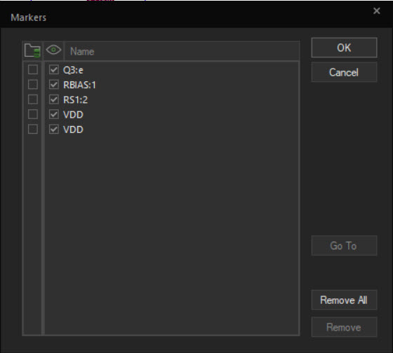
You can also access the Markers dialog box by choosing PSpice – Markers – List from the Capture main menu.
2. Deselect the extra markers.
3. Click OK.
4. Run PSpice icon ( ) to start the simulation.
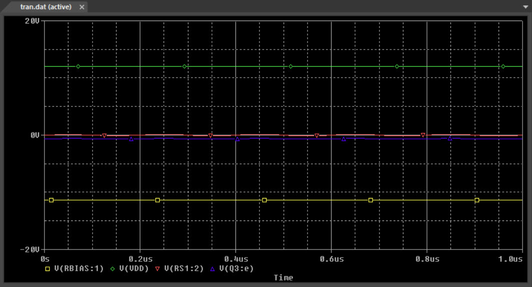
The simulation starts, and you can see the waveform in PSpice.
The deselected markers in the Markers dialog box appear in gray, as shown in the following figure:
Identify Marker as Special
You can also restrict an additional marker from being used for data collection during the simulation run by assigning the marker as special using the following steps:
- Click Cancel in the message box.
- On the schematic, select the extra markers.
- Right-click and choose Mark Special.
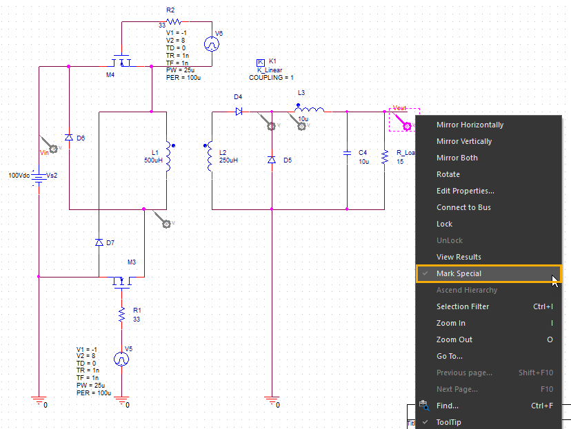
4. Next, click the Run PSpice icon () to start the simulation.
Utilizing Unused Markers for Data Collection
You can make use of the unused markers in a design, by doing the following steps:
- Right-click any additional marker added that is marked as special.
- Deselect Mark Special.
- Repeat step 1-2 for any other unused markers.
- At any point, ensure that the number of active markers for data collection is not more than four and then run the simulation.
Model Parameters for Specific Devices
You can edit model parameters for the following devices and plot all the waveforms for your simulation circuit.
- Passives: R, L, C, K
- Switches: S, W
- Transmission line: T
- Digital stimulus: U - STIM
- Independent sources: V, I
- Controlled sources: E, F, G, H
- Subcircuit: X
For other device types, after editing the models you can plot up to four markers.
Simulation Netlist
When generating a PSpice netlist, you can choose between two types of netlist formats:
- Flat netlist
- Hierarchical netlist
Use the PSpice tab on the Create Netlist dialog box to generate a customized PSpice netlist.
Viewing Simulation Netlist
You can view the most recent simulation netlist for a selected design, or the current design.
To view a simulation netlist:
- In the project manager, select the design for which you want to create a netlist, or open a schematic page.
- From the PSpice menu, choose View Netlist.
Running a Simulation
You can simulate your Capture design using PSpice, provided that there are PSpice models for the parts in your design. PSpice and Capture are fully integrated.
To run a simulation:
- In the project manager, select a design to simulate, or open a schematic page.
- In the project manager, select a simulation profile.
- From the PSpice menu, choose Run or press the F11 function key.
PSpice does the following:
- Checks design rules for your design.
- Creates a simulation netlist for PSpice.
- Opens PSpice using the netlist created from your design.
PSpice creates an output file (.OUT) as the simulation progresses. It contains bias point information, model parameter values, error messages, and so on. If the simulation fails, you can view the output file to see the error messages.
If the simulation completes successfully, PSpice produces a data file (.DAT). This is the file PSpice uses to display the simulation results. To see marker simulation results, the schematic must be open.
Viewing Simulation Results
You can view results as a simulation progresses or after a simulation is completed. At any point you can also view the most recent simulation results or view the output file (.out).
Viewing Results of Simulation Progress
To view results as a simulation progresses, do the following:
- From the PSpice menu, choose Edit Simulation Settings.
The Simulation Settings dialog box appears. - In the Probe Window tab, select the Display Probe window check box.
- Select the during simulation option.
- Click OK.
Viewing the Most Recent Simulation Results
You can view the most recent simulation results for a schematic. If the schematic was simulated with more than one profile, you can choose which profile results to view.
To view the most recent simulation results, do the following:
- Open the schematic for which you want to view simulation results.
You must do this to see marker results. - In the project manager, select the simulation profile you want to be active.
- From the PSpice menu, choose View Simulation Results, or press the
F12function key.
Viewing Output File
To view the most recent output file, do the following:
- In the project manager, choose the simulation profile for which you want to see the output file.
- From the PSpice menu, choose View Output File.
Editing Simulation Settings
Simulation profiles can be edited in Capture and PSpice.
To edit simulation settings from Capture
- Choose PSpice – Edit Simulation Settings. The Simulation Settings dialog box appears.
- Click the tab for the settings you want to change.
- Edit the settings and click Apply.
- Repeat steps 2 and 3 until you have changed all the settings you need.
- Click OK.
Shortcut
Keyboard: ALT+S+E
Placing Markers
To view the markers in the simulation results, the schematic must be open.
To place markers in your design:
- From the PSpice menu, choose Markers.
- Select the marker you want to place.
- Drag the marker symbol attached to the cursor to the location where you want to place it.
- Click to place the symbol.
- Repeat steps 3 and 4 until you have that you want.
- Press the Esc key to end the marker mode, or right-click and select the End Mode.
Changing Visibility of Markers
You can show all, hide all, or delete all markers. Showing or hiding markers in the schematic also shows or hides the trace results in the Probe window.
To show all, hide all, or delete all markers:
- Choose the PSpice – Markers menu command.
- Select the Show All, Hide All, or Delete All option.
Simulating and Viewing Results of Multiple Profiles
You can select one profile or multiple profiles to be simulated or viewed. If you select only a single profile for simulation, it is handled as though you selected the Run command. If you select a file for viewing, it is handled as though you chose the View Simulation Results command.
If you select multiple profiles, simulations for all selected profiles are performed using the simulation queue. You must then open the .DAT files to view the results.
To simulate multiple profiles, do the following:
- In the project manager, choose the simulation profiles you want to simulate.
- From the PSpice menu, choose Simulate Selected Profile(s).
PSpice opens and processes the profiles using the simulation queue.
To view the results, do the following:
- Close the simulation queue, but leave PSpice active.
- The Probe window is active, but no traces are visible.
- From the PSpice File menu, choose Open.
- Select the
.DATfiles that you want to view and click the Open button.
A tab for each of the.DATfiles you selected appears at the bottom of the Probe window. - From the PSpice Window menu, choose Display Control.
- Select a profile for which you want to display the results.
- Click Restore.
- Repeat steps 4, 5, and 6 for all the profiles you want to view.
You can then click each tab to view the displayed results.
Making a Simulation Profile Active
To simulate a design with a specific simulation profile, or to view the most recent results of a specific simulated profile, you must activate the profile.
To activate a simulation profile, do the following:
- In the project manager, choose the simulation profile you want to activate.
- From the PSpice menu, choose Make Active.
Files Needed for Simulation
To simulate your design, PSpice needs to know about:
- parts in your circuit and how they are connected,
- what analysis to run,
- the simulation models that correspond to the parts in your circuit, and
- the simulation models that correspond to the parts in your circuit, and
- the stimulus definitions with which to test.
This information is provided in various data files.
Some of these are generated by the design entry program such as Capture , others come from libraries , and still others are user-defined.
Files that Design Entry Programs generate
When you begin the simulation process, the design entry programs first generate files describing the parts and connections in your circuit. These files are the netlist file and the circuit files that PSpice reads before doing anything else.
Netlist file
The netlist file contains a list of device names, values, and how they are connected with other devices. The name that design entry program generate for this file is DESIGN_NAME-DESIGN_NAME.NET. The netlist file is located in the directory:
<project_directory>\worklib\<design_name>\cfg_analog\
Other files that you can configure for simulation
Before starting simulation, PSpice needs to read other files that contain simulation information for your circuit. These are model files, and if required, stimulus files and include files.
The simulation profile contains references to the other user-configurable files that PSpice needs to read.
You can create these files using PSpice programs like the Stimulus Editor and the Model Editor. These programs automate file generation and provide graphical ways to verify the data. You can also use the Model Text view in the Model Editor (or another text editor like Notepad) to enter the data manually.
Model library
PSpice uses this information in a model library to determine how a part will respond to different electrical inputs. These definitions take the form of either a:
- model parameter set, which defines the behavior of a part by fine-tuning the underlying model built into PSpice
- or a subcrcuit netlist, which describes the structure and function of the part by interconnecting other parts and primitives.
The most commonly used models are available in the PSpice model libraries shipped with your programs. The model library names have a.LIB extension.
If needed, however, you can create your own models and libraries, by:
- manually using the Model Text view in the Model Editor (or another text editor like Notepad),
or
- automatically using the Model Editor.
Stimulus file
You can create a stimulus file by:
- manually using the text editor in PSpice (or a standard text editor) to create the definition (a typical file extension is .STM)
- or -
- automatically using the Stimulus Editor (which generates an .STL file extension).
Include file
An include file is a user-defined file that contains:
- PSpice commands,
- supplemental text comments that you want to appear in the PSpice output file.
You can create an include file using any standard text editor. Typically, include file names have a .INC extension.
An include file can contain definitions, using the PSpice .FUNC command, for functions that you want to use in numeric expressions elsewhere in your design.
Configuring model library, stimulus, and include files
PSpice searches model libraries, stimulus files, and include files for any information it needs to complete the definition of a part or to run a simulation.
The files that PSpice searches depend on how you configure your model libraries and other files. Much of the configuration is set up for you automatically, however, you can do the following yourself:
- Add and delete files from the configuration.
- Change the scope of a file: that is, whether the file applies only to a profile, a design (local) or to any design (global).
- Change the search order.
To configure these, edit the simulation profile by using the Configuration Files tab in the Simulation Settings dialog box.
Files that PSpice generates
After reading the circuit file, netlist file, model libraries, and any other required inputs, PSpice starts the simulation. As simulation progresses, PSpice saves results to two files--the data file and the PSpice output file.
Probe data file
The data file contains simulation results that can be displayed graphically. PSpice reads this file automatically and displays waveforms reflecting the circuit response at nets, pins, and parts that you marked in your design (cross-probing). You can set up your simulation so that PSpice displays the results as the simulation progresses or after the simulation completes.
After PSpice has read the data file and displayed the initial set of results, you can add more waveforms and perform post-simulation analysis of the data.
There are two ways to add waveforms to the display:
- From within PSpice, by specifying trace expressions.
- From within the design entry program, by cross-probing.
PSpice output file
The PSpice output file is an ASCII text file that contains:
- the netlist representation of the circuit
- the PSpice command syntax for simulation commands and options (like the enabled analyses)
- simulation results
- warning and error messages for problems encountered during read-in or simulation
Its content is determined by:
- the types of analyses you run
- the options you select for running PSpice
- the simulation control parts (like VPRINT1 and VPLOT1) that you place and connect to nets in your design
Running PSpice in Batch Mode
Simulations in PSpice can be run in batch mode.
Interactive Mode
In this mode, PSpice is invoked from the command line, and the simulation circuit file is loaded. For information on the command-line options, see the PSpice Reference Guide.
To run a set of simulation circuit files (*.cir), the following command can be used on the Windows command prompt:
<path to pspice.exe/pspice.exe /r <path to cir file>
For example:
<CDS_INST_DIR>\tools\pspice\pspice.exe /r C:/mysim/test1.cir
To set up multiple simulations, a batch file can be created with each command calling a different .cir file.
Non-Interactive Mode
In this mode, the simulation runs in the background and PSpice is not invoked. To run this, the psp_cmd.exe executable is called from the command line. This executable resides in the same location as pspice.exe. For example:
<CDS_INST_DIR>\tools\pspice\psp_cmd.exe /r <path to cir file>
The background simulation has the advantage that in case of non-convergence, it waits for user intervention for 10 seconds, and if no action is taken, it proceeds to the next available command.
SPICE netlist format
Generic, flat SPICE format netlists have the following characteristics:
- Part names, module names, reference strings, node names, and pin numbers are not checked for length.
- Node numbers are limited to five characters.
- If the Use net names option is selected, legal characters for node names are limited to:
0..9 A..Z a..z $ _ (underscore)
If you select this option, Capture uses the node names you placed on the schematic page (via aliases and hierarchical ports), where available. Not all versions of SPICE support alphanumeric node names. Check your SPICE manual for details. If your version of SPICE does not allow alphanumeric node names, you can still give them numeric names such as "17." These numeric names do not interfere with the ones generated by Capture, since the node numbers it generates begin at 10000 (except GND, which is always 0).
- All ASCII characters are legal except as noted for node names.
For more information on flat SPICE netlists, see the flat SPICE netlist example.
The Spice formats
Capture provides two SPICE netlist formats. The first format produces either hierarchical or flat netlist output, depending on your project structure and the active view. It is accessible from the SPICE tab on the Create Netlist dialog box. The second format produces only flat netlists, and is accessible through the Other tab on the Create Netlist dialog box.
Use the SPICE tab if:
- You want to include net, part, and pin properties.
- You want a hierarchical netlist.
Use the Other tab if: - You want a flat netlist of a simple hierarchical design.
Hierarchical designs in SPICE
For hierarchical designs, the SPICE format produces netlists with subcircuit (.SUBCKT) definitions for schematic pages in the hierarchy. These subcircuits are called by the X command (subcircuit call). Since SPICE does not require subcircuits to be defined before use, the hierarchy appears in normal form in the netlist with the root page at the top of the file.
According to the PSPICE manual, the X subcircuit general form is:
X name [nodes] subcircuit-name
where:
name Specifies a unique name for the device
nodes Specifies the list of nets that attach to the device in the same order as the .SUBCKT definition used by the device
subcircuit-name Specifies the name of a .SUBSCKT definition that the X device uses
The following is an example of an X subcircuit call:
XBUF 13 15 UNITAMP
For more information on hierarchical SPICE netlists, see the hierarchical SPICE netlist example.
SPICE netlist constraints
- Capture can create netlists larger than what most PC-based SPICE programs accept. Consult your SPICE manual for the limits. If your PC meets SPICE's memory requirements, you can generate the largest allowed netlist.
- The part value is used to pass modeling information to the netlist. For instance, resistor RS1 in the example flat schematic folder has a value of 1K Ohms; in the example hierarchical schematic folder R1 has a value of 6.8K Ohms.
- Use the special PSPICE.OLB or SPICE.OLB libraries supplied by OrCAD when generating a SPICE netlist. These libraries already have pin numbers on the parts and are compatible with most versions of SPICE. The PSPICE.OLB contains many specific part types, such as a 2N2222 NPN transistor, that are not provided in the generic SPICE.OLB.
- All library part pin names should be changed to reflect the model node index. To find out the proper node ordering, see your SPICE manual.
As an example of what to change, the OrCAD-supplied NPN transistor has the pin names defined as base, emitter, and collector in the DEVICE.OLB library. For SPICE to understand the nodal information, the pin names must be changed from base, emitter, and collector to 2, 3, and 1 (as defined in the SPICE manual). Therefore, the library source file for an NPN transistor that is compatible with the SPICE pin numbering convention is as follows:
 'NPN'
 REFERENCE 'Q'
 {X Size =} 2 {Y Size =} 2 {Parts per Package =} 0
 L1 SHORT IN '2'
 B2 SHORT IN '3'
 T2 SHORT IN '1'
 { 0}..##.#
 { 1} ## #
 .
 .
 .
SPICE map files
In addition to the netlist file, Capture also creates a map file when you select the SPICE format. The node numbers created by Capture are placed in the .MAP file so you can cross-reference the SPICE node numbers with the node names that you specified on your schematic page. You must enter the map filename in the Map File text box in the Create Netlist dialog box.
If you select the Use net names option, the map file may contain erroneous results.
For more information on SPICE map files, see the flat and hierarchical map file examples.
SPICE pipe commands
You can place lines of text on your schematic page to be included in the SPICE netlist. Select the Text command on the Place menu to place the text on your schematic page.
Each line of text must start with the pipe character (|). The first line must be:
|SPICE
This tells Capture to extract the information in the following lines of text when generating a SPICE netlist. The remaining lines can contain any information you want to include in the netlist. The lines following |SPICE are placed at the top of the netlist.
Defining Stimuli
To simulate your circuit, you need to connect one or more source parts that describe the input signal that the circuit must respond to .
The PSpice libraries supply several source parts that are described in the tables that follow. These parts depend on:
- the kind of analysis you are running,
- whether you are connecting to the analog or digital portion of your circuit, and
- how you want to define the stimulus: using the Stimulus Editor, using a file specification, or by defining part property values.
Analog stimuli
Analog stimuli include both voltage and current sources. The following table shows the part names for voltage sources.
| Input | Part for voltage |
|---|---|
| DC bias | VDC or VSRC |
| AC magnitude and phase | VAC or VSRC |
| exponential | VEXP or VSTIM |
| periodic pulse | VPULSE or VSTIM |
| piecewise-linear | VPWL or VSTIM |
| piecewise-linear that repeats forever | VPWL_RE_FOREVER or VPWL_F_RE_FOREVER |
| piecewise-linear that repeats n times | VPWL_N_TIMES or VPWL_F_N_TIMES* |
| frequency-modulated sine wave | VSFFM or VSTIM |
| sine wave | VSIN or VSTIM |
*VPWL_F_RE_FOREVER and VPWL_F_N_TIMES are file-based parts; the stimulus specification is saved in a file and adheres to the PSpice netlist syntax.
To determine the part name for an equivalent current source, in the table of voltage source parts, replace the first V in the part name with I. For example, the current source equivalent to VDC is IDC, to VAC is IAC, to VEXP is IEXP, and so on.
Using VSTIM and ISTIM
You can use VSTIM and ISTIM parts to define any kind of time-based input signals.
To specify the input signal itself, you need to use the Stimulus Editor.
Specifying multiple stimulus types
If you want to run more than one analysis type, including a transient analysis, then you need to use either of the following:
- time-based stimulus parts with AC and DC properties
- VSRC or ISRC parts
Using time-based stimulus parts with AC and DC properties
The time-based stimulus parts that you can use to define a transient, DC, and/or AC input signal are listed below.
| VEXP | IEXP |
| VPULSE | IPULSE |
| VPWL | IPWL |
| VPWL_F_RE_FOREVER | IPWL_F_RE_FOREVER |
| VPWL_F_N_TIMES | IPWL_F_N_TIMES |
| VPWL_RE_FOREVER | IPWL_RE_FOREVER |
| VPWL_RE_N_TIMES | IPWL_RE_N_TIMES |
| VSFFM | ISFFM |
| VSIN | ISIN |
In addition to the transient properties, each of these parts also has a DC and AC property. When you use one of these parts, you must define all of the transient properties. However, it is common to leave DC and/or AC undefined (blank). When you give them a value, the syntax you need to use is as follows.
| Property | Syntax |
|---|---|
| DC | DC_value[units] |
| AC | magnitude_value[units] [phase_value] |
Using VSRC or ISRC parts
The VSRC and ISRC parts have one property for each analysis type: DC, AC, and TRAN. You can set any or all of them using PSpice netlist syntax. When you give them a value, the syntax you need to use is as follows.
| Property | Syntax |
|---|---|
| DC | DC_value[units] |
| AC | magnitude_value[units] [phase_value] |
| TRAN | time-based_type (parameters) |
where time-based_type is EXP, PULSE, PWL, SFFM, or SIN, and the parameters depend on the time-based_type.
Digital stimuli
| Input | Part |
|---|---|
| For transient analyses | |
| DIGSTIMn | signal or bus (any width) |
| DIGCLOCK | clock signal |
| STIM1 | 1-bit signal |
| STIM4 | 4-bit bus |
| STIM8 | 8-bit bus |
| STIM16 | 16-bit bus |
| FILESTIMn | file-based signal or bus (any width) |
Importing PSpice Schematic Projects in Capture
You can import a MicroSim Schematics project to a Capture project.
To convert a Schematics project to Capture:
- In Capture, choose File – Import – PSpice.
The Import Design dialog box opens.
- In the PSpice tab, select the source schematic (Open), the destination project, (Save As) and the PSPICE.INI (Schematic Configuration File) file for existing settings.
-
Click OK to start the automated translation utility.
Viewing Information on Missing PSpice Models in Online DRC
For a part placed on the schematic, if the PSpice model associated with the part is not found in the configured libraries, information related to such a part instance appears as a message in the Online DRC tab of the Output pane.

Viewing PSpice Models within Capture
Capture provides a dedicated and in-built view of the PSpice models. For a part placed on the schematic, you can view the information of its associated PSpice model in a separate tab in the canvas area.
- To do so, right-click a part and choose View PSpice Model.
This information is read-only. Some of the information may be non-readable if the associated model is encrypted.
Associating PSpice Model to Capture Parts
You can associate a PSpice model to an existing or new part created in Capture. Before associating a PSpice model to a part, ensure the following:
-
Use this feature on a part placed on the root schematic. If the design is not a root schematic, open the project manager, right-click this schematic, and select Make Root to convert it into a root schematic design.
- Only a single part should be selected at a time.
- PSpice models can only be associated with homogeneous parts.
- If the PSpice model is to be associated to a part in an externally referenced design, you need to open this design separately. Next, associate a PSpice model to the required part, save the design and then reuse it in the root schematic.
To associate a PSpice model to a Capture part in the schematic editor:
-
Select the Capture part to which you want to associate a PSpice model.
-
Select Tools – Associate PSpice Model.
or
Right-click the part and choose Associate PSpice Model. -
A message appears prompting you to save the design before model association. If the selected part already has an associated model, a message appears to confirm if you want to overwrite this implementation. Click Yes.
The Associate PSpice Model dialog box appears.
 If the symbol is open in Capture, the Associate PSpice Model option will appear disabled in the pop-up menu.
 - Click Browse to specify the name and location of the library containing the required PSpice model. You can either select the library from the Model Library drop-down list box or browse to the library location.
- Once you have selected the
.libfile, the Associate PSpice Model window lists the matching models. By default, the Show matching models option is selected. To view all the models, select the Show all models option.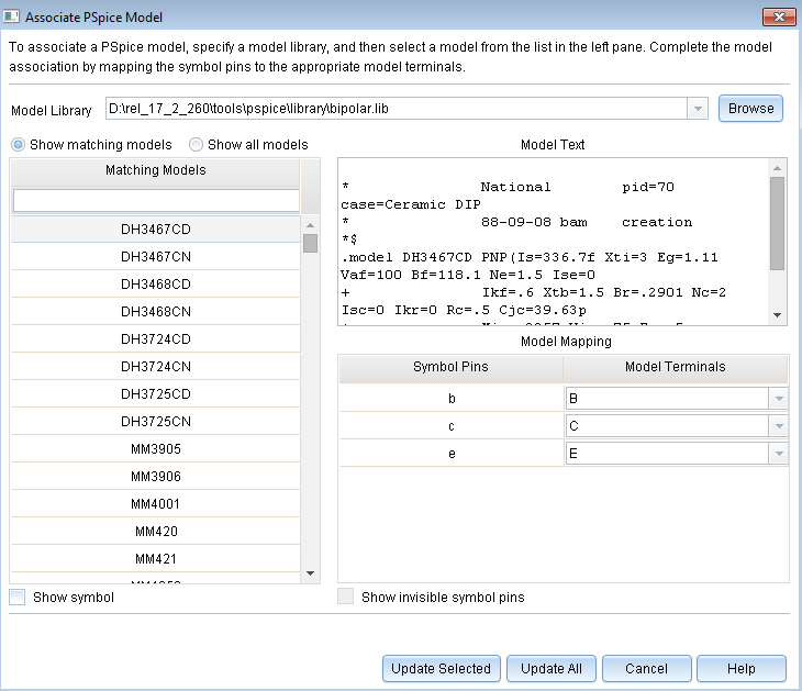
- Select the required model from the Matching Models section.
-
Map each symbol pin to the correct model terminal in the Model Mapping section. The model terminals for the selected symbol pins appear in the Model Terminals drop-down list.
For mapping, you can view the model definition. When you select a model in the Matching Models section, its definition appears in the Model Text section.
Click the Show symbol check box to preview the symbol along with its sections. The symbol preview can only be seen when the library path specified in Design Cache exists.

-
Select the Show invisible symbol pins check box to view and map any invisible power pins in the symbol. This check box will appear disabled if there are no such pins.
-
Click Update Selected to complete attaching the selected PSpice model to the selected Capture part and to close the Associate PSpice Model window. A message appears to indicate that the selected model is now attached to the part selected on the schematic editor.
 Update All
If you click Update All, all part instances of the same source package are associated with the selected PSpice model. if you click Update All, and the selected part is also in an externally referenced design, the PSpice model will not be associated to such a part.
- Click OK.
This automatically saves the design.
Global Parameters and Expressions
In addition to literal values, you can use global parameters and expressions to represent numeric values in your circuit design.
Global parameters
A global parameter is like a programming variable that represents a numeric value by name.
Once you have defined a parameter (declared its name and given it a value), you can use it to represent circuit values anywhere in the schematic; this applies to any hierarchical level.
Some ways that you can use parameters are as follows:
- Apply the same value to multiple part instances.
- Set up an analysis that sweeps a variable through a range of values (for example, the DC sweep or parametric analysis).
When multiple parts are set to the same value, global parameters provide a convenient way to change all their values for "what-if" analyses.
For example, if two independent sources have a value defined by the parameter VSUPPLY, then you can change both sources to 10 volts by assigning the value once to VSUPPLY.
Declaring and using a global parameter
To use a global parameter in your design, you need to:
- define the parameter using a PARAM part from SPECIAL.OLB.
- use the parameter in place of a literal value somewhere in your design.
To declare a global parameter
- Place a PARAM part in your design.
- Double-click the PARAM part to display the Parts spreadsheet.
- Do the following for each global parameter:
- Click New, then enter NAMEn in the Property Name field, then click OK. This creates a new property for the PARAM part, NAMEn in the spreadsheet.
- Click on the cell below the NAMEn column and enter a default value for the parameter.
- While this cell is still selected, click Display. In the Display format frame, select Name and Value, then click OK.
System variables have reserved parameter names. Do not use these parameter names when defining your own parameters.
- Click Apply to update all the changes to the PARAM part, and then close the spreadsheet.
For example, to declare the global parameter VSUPPLY that will set the value of an independent voltage source to 14 volts, place the PARAM part, and then create a new property named VSUPPLY with a value of 14V.
To use the global parameter in your circuit
- Find the numeric value that you want to replace: a component, model parameter, or other property value.
- Replace the value with the name of the global parameter using the following syntax:
{ global_parameter_name }
The curly braces tell PSpice to evaluate the parameter and use its value.To avoid errors, always include parameter variable name in curly braces when it is assigned to the parameter/property on the part.
Expressions
PSpice evaluates the expression to a single value every time:
- it reads in a new circuit
- a parameter value used within an expression changes during an analysis.
An example of this would be a parameter that changes with each step of a DC sweep or parametric analysis.
Specifying expressions
To use an expression in your circuit
- Find the numeric or boolean value you want to replace: a component value, model parameter value, other property value, or logic in an IF function test.
- Replace the value with an expression using the following syntax:
{expression }
where {expression} can contain any of the following:- standard operators (listed in the table below)
- built-in functions (listed in the PSpice User Guide)
- user-defined functions
- system variables (listed in the PSpice User Guide)
- user-defined global parameters
- literal operands
The curly braces tell PSpice to evaluate the expression and use its value.
| Operator class | Operator | Operation |
|---|---|---|
| arithmetic | ||
| + | addition or string concatenation | |
| - | subtraction | |
| * | multiplication | |
| / | division | |
| ** | exponentiation | |
| logical | ||
| ~ | unary NOT | |
| | | boolean OR | |
| ^ | boolean XOR | |
| & | boolean AND | |
| relational* | ||
| == | equality test | |
| != | non-equality test | |
| > | greater than test | |
| >= | greater than or equal to test | |
| < | less than test | |
| <= | less than or equal to test |
*Logical and relational operators are used within the IF() function; for digital parts, logical operators are used in Boolean expressions.
Using the FLOAT Property for Unconnected Pins
When preparing a circuit for simulation with PSpice, it is important that all pins for all parts are connected properly. If a pin is meant to remain unconnected intentionally, you need to use the PSpice pin property FLOAT, rather than a No Connect symbol. Otherwise, the circuit may not netlist correctly for PSpice.
The pin property FLOAT may have one of the following three values:
| Value | Description |
|---|---|
| Error | The pin will not netlist. An error message will be returned when the PSpice simulation netlist is generated. Use Error when you want to be reminded that this pin is a "no connect" and should be treated in a special way. Error is the default value. |
| RtoGND | The pin is connected to a virtual resistor, whose opposite pin is tied to GND. The resistor has a value of 1/GMIN. This value allows the simulation netlist to be created and allows PSpice to perform the analysis. The virtual resistor will not be processed as part of a layout netlist or appear in a BOM. |
| UniqueNet | The pin, when left unconnected, is attached to a unique node when the PSpice simulation netlist is generated. Use UniqueNet when you want the pin to remain unconnected but correspond to the Probe data associated with its part. |
The FLOAT property can either be defined in the part editor when creating a new part, or you can edit a pin on an existing part using the property editor.
To define the FLOAT property using the property editor
- In Capture, double-click on the pin to open the property editor spreadsheet.
- Click on the Pins tab.
- Click New Property and type FLOAT (upper case) in the Name text box.
- Type the property value you want to use, then click OK.
- Click Apply or close the spreadsheet to have the changes take effect.
Placing PSpice Ground 0 Symbols for PSpice Simulations
For PSpice analog simulation to run, your design must have a PSpice ground (0) symbol. The CAPSYM.OLB, which is the default library in Capture, includes the PSpice ground (0) symbol. Use the 0 symbol to place a PSpice ground 0 symbol in your design.
To select the 0 symbol, do the following:
- Choose Place – Ground (or use the Place Ground toolbar button). The Place Ground dialog box appears.
-
Select the CAPSYM part library from the Libraries list (if it is not already selected).
You can also place the 0 symbol from the Source part library. To do this, add the Source part library to the Libraries list using the Add Library button; SOURCE.OLB is located in the \TOOLS\CAPTURE\LIBRARY\PSPICE subdirectory under your installation directory.
- Select the 0 symbol (if not already selected).
-
Click OK to place the PSpice ground 0 symbol.
Alternatively:
- You can place any ground symbol, open the Property Editor, and change its name to 0.
- You can place PSpice ground 0 symbol from PSpice Component quick pick, that is, Place - PSpice Component - PSpice Ground.
Guidelines and Best Practices for Specifying Values for Part Properties
Note the following when specifying values for part properties:
- Do not leave a space between the value and its unit, if the unit is a scale symbol. For example, specify 5K instead of 5 K.
- You can use the European notation, where the decimal point is omitted and replaced by the unit symbol, for specifying values. For example, you can use 3K3, which is the European notation for 3.3K.
- Specify tolerance values as percentages. If you specify an absolute value, the tolerance value will be read as an absolute number. For example, if you specify the value of the POSTOL property as a percentage, say 10%, on a 10K resistor, the distribution values will be taken in the range of 10K?1K. If you specify the tolerance value as an absolute number, say 10, the distribution values will be taken in the range of 10K?10?
- Do not add any space for the name of an hierarchical block.
Defining Part Properties Needed for Simulation
Passive Parts
The PSpice libraries supply several basic parts based on the passive device models built into PSpice. These are summarized in the following table.
To find out more about how to use these parts and define their properties, look up the corresponding PSpice device letter in the Analog Devices chapter in the online PSpice Reference Manual, and then see the Capture Parts sections.
| Available Parts | Device Type | PSpice Device Letter... |
|---|---|---|
| C C_VAR | capacitor | C |
| L | inductor | L |
| R R_VAR | resistor | R |
| XFRM_LINEAR K_LINEAR | transformer | K and L |
| T | ideal transmission line | T |
| TLOSSY | Lossy transmission line | T |
| TnCOUPLED TnCOUPLEDX* KCOUPLEn* | coupled transmission line | T and K |
*For these device types, the PSpice libraries supply several parts. Refer to the online PSpice Reference Manual for the available parts.
Breakout Parts
The PSpice libraries supply passive and semiconductor parts with default model definitions that define a basic set of model parameters. This way, you can easily:
- assign device and lot tolerances to model parameters for Monte Carlo and sensitivity/worst-case analyses
- define temperature coefficients
- define device-specific operating temperatures
These are called breakout parts and are summarized in the following table.
| Breakout Part | Device Type | PSpice Device Letter |
|---|---|---|
| BBREAK | GaAsFET | B |
| CBREAK | capacitor | C |
| DBREAKx | diode | D |
| JBREAKx* | JFET | J |
| KBREAK | inductor coupling | K |
| LBREAK | inductor | L |
| MBREAKx* | MOSFET | M |
| QBREAKx* | bipolar transistor | Q |
| RBREAK | resistor | R |
| SBREAK | voltage-controlled switch | S |
| TBREAK | transmission line | T |
| WBREAK | current-controlled switch | W |
| XFRM_NONLINEAR | transformer | K and L |
| ZBREAKN | IGBT | Z |
* For this device type, the PSpice libraries supply several breakout parts. Refer to the online PSpice Reference Manual for the available parts.
Behavioral Parts
Behavioral parts allow you to define how a block of circuitry should work without having to define each discrete component.
Analog behavioral parts
These parts use analog behavioral modeling (ABM) to define each part's behavior as a mathematical expression or lookup table. The PSpice libraries provide ABM parts that operate as math functions, limiters, Chebyshev filters, integrators, differentiators, and others that you can customize for specific expressions and lookup tables. You can also create your own ABM parts.
Digital behavioral parts
These parts use special behavioral primitives to define each part's functional and timing behavior. These primitives are:
| LOGICEXP | to define logic expressions |
| PINDLY | to define pin-to-pin delays |
| CONSTRAINT | to define constraint checks |
Many of the digital parts provided in the PSpice libraries are modeled using these primitives. You can also create your own digital behavioral parts using these primitives.
If you want to use a part for simulation, then your part should have the PSPICETEMPLATE property defined for it:
You can also add other simulation-specific properties for digital parts: IO_LEVEL, MNTYMXDLY, and PSPICEDEFAULTNET.
Here are the things to check when editing part properties:
- Does the property specify the correct number of pins/ nodes?
- Are the pins/ nodes in the specified property in the proper order?
- Do the pin/ node names in the property match the pin names on the part?
For examples of how to use the property, see PSPICETEMPLATE examples.
PSPICETEMPLATE property
The PSPICETEMPLATE property defines the PSpice syntax for the part's netlist entry. When creating a netlist, Capture substitutes actual values from the circuit into the appropriate places in the PSPICETEMPLATE syntax, then saves the translated statement to the netlist file.
Any part that you want to simulate must have a defined PSPICETEMPLATE property. These rules apply:
- The pin names specified in the PSPICETEMPLATE property must match the pin names on the part.
- The number and order of the pins listed in the PSPICETEMPLATE property must match those for the associated .MODEL or .SUBCKT definition referenced for simulation.
- The first character in a PSPICETEMPLATE must be a PSpice device letter appropriate for the part (such as Q for a bipolar transistor).
PSPICETEMPLATE syntax
The PSPICETEMPLATE contains:
- regular characters that the schematic page editor interprets verbatim, and
- property names and control characters that the schematic page editor translates.
Regular characters in template
Regular characters include the following:
- alphanumeric
- any keyboard part except the special syntactical parts used with attributes (@ & ? ~ #)
- whitespace
An identifier is a collection of regular characters of the form:
alphabetic character [any other regular character]*.
Property names in templates
Property names are preceded by a special character as follows:
[ @ | ? | ~ | # | & ]<identifier>
The schematic page editor processes the property according to the special character as shown in the following table.
| Syntax* | Replacement |
|---|---|
| @<id> | Value of <id>. Error if no <id> property or if no value assigned. |
| &<id> | Value of <id>, if <id> is defined. |
| ?<id>s...s | Text between s...s separators, if <id> is defined. |
| ?<id>s...ss...s | Text between the first s...s separators, if <id> is defined, else the second s...s clause. |
| ~<id>s...s | Text between s...s separators, if <id> is undefined. |
| ~<id> s...ss...s | Text between the first s...s separators, if <id> is undefined, else the second s...s clause. |
| #<id>s...s | Text between s...s separators, if <id> is defined, but delete rest of template if <id> is undefined. |
*s is a separator character.
Separator characters include commas (,), periods (.), semi-colons (;), forward slashes (/), and vertical bars ( | ). You must always use the same character to specify an opening-closing pair of separators.
The caret (^) character in templates
The schematic page editor replaces the caret (^) character with the complete hierarchical path to the device being netlisted.
The new line (\n) character sequence in templates
The part editor replaces the new line (\n) character sequence with a new line. Using newline character sequence (\n), you can specify a multiline netlist entry from a one-line template.
The percentage (%) character and pin names in templates
Pin names are denoted as follows:
%<pin name>
where pin name is one or more regular characters.
The schematic page editor replaces the %<pin name> clause in the template with the name of the net connected to that pin.
The end of the pin name is marked with a separator. To avoid name conflicts in PSpice, the schematic page editor translates the following characters contained in pin names.
| Pin name character | Replacement |
|---|---|
| < | l (L) |
| > | g |
| = | e |
| \XXX\ | XXXbar |
Templates for devices in the part library start with a PSpice device letter, followed by the hierarchical path, and then the reference designator (REFDES) property. We recommend that you adopt this scheme when defining your own netlist templates.
PSPICETEMPLATE examples
Simple resistor (R) template
The R part has two pins (1 and 2) and two required properties, REFDES and VALUE.
The template for the resistor is:
R^@REFDES %1 %2 @VALUE
A sample translation of the template is:
R_R23 abc def 1k
where REFDES equals R23, VALUE equals 1k, and R is connected to nets abc and def.
Voltage source with optional AC and DC specifications (VAC) template
The VAC part has two properties, AC and DC, and two pins, + and -.
The template is:
V^@REFDES %+ %- ?DC|DC=@DC| ?AC|AC=@AC|
A sample translation of the template is:
V_V6 vp vm DC=5v
where REFDES equals V6, VSRC is connected to nodes vp and vm, DC is set to 5v, and AC is undefined.
Another sample translation of the template is:
V_V6 vp vm DC=5v AC=1v
where, in addition to the settings for the previous translation, AC is set to 1v.
Parameterized subcircuit call (X) template
This example supposes a subcircuit Z that has two pins (a and b) and a subcircuit parameter G, where G defaults to 1000 when no value is supplied.
To allow the parameter to be changed on the schematic page, treat G as property in the template.
The template is:
X^@REFDES %a %b Z PARAMS: ?G|G=@G|
~G|G=1000|
An equivalent template (using the if...else form) is:
X^@REFDES %a %b Z PARAMS: ?G|G=@G||G=1000|
A sample translation of the template is:
X_U33 101 102 Z PARAMS: G=1024
where REFDES equals U33, G is set to 1024, and the subcircuit connects to nets 101 and 102.
Another sample translation of the template is:
X_U33 101 102 Z PARAMS: G=1000
where the settings of the previous translation apply except that G is undefined.
Digital stimulus parts with variable width pins template
For a digital stimulus device template (such as that for a DIGSTIM part), a pin name can be preceded by an asterisk (*) character. This signifies that the pin can be connected to a bus and the width of the pin is set to be equal to the width of the bus.
The template is:
U^@REFDES STIM(%#PIN, 0) %*PIN
\n+ STIMULUS=@STIMULUS
where #PIN refers to a variable width pin.
A sample translation of the template is:
U_U1 STIM(4,0) 5PIN1 %PIN2 %PIN3 %PIN4
+ STIMULUS=mystim
where the stimulus is connected to a four-input bus, a[0-3].
Pin callout in subcircuit templates
The number and sequence of pins named in a template for a subcircuit must agree with the definition of the subcircuit itself--that is, the node names listed in the .SUBCKT statement, which heads the definition of a subcircuit. These are the pinouts of the subcircuit.
IO_LEVEL property
The IO_LEVEL property defines the level of interface subcircuit model PSpice must use for a digital part that is connected to an analog part.
If you are creating a digital part, you need to
-
Add the IO_LEVEL property to the part and assign a value shown in the table below.
Value Interface subcircuit (level) 0 circuit-wide default 1 AtoD1 and DtoA1 2 AtoD2 and DtoA2 3 AtoD3 and DtoA3 4 AtoD4 and DtoA4 - Use this property in the property definition (IO_LEVEL is also a subcircuit parameter used in calls for digital subcircuits).
MNTYMXDLY property
The MNTYMXDLY property defines the digital propagation delay level that PSpice must use for a digital part.
If you are creating a digital part, you need to do the following
-
Add the MNTYMXDLY property to the part and assign a value shown in the table below.
Value Propagation delay 0 circuit-wide default 1 minimum 2 typical 3 maximum 4 worst-case (min/max) - Use this property in the property definition (MNTYMXDLY is also a subcircuit parameter used in calls for digital subcircuits).
PSPICEDEFAULTNET property
The PSPICEDEFAULTNET pin property defines the net name to which a power or ground (invisible) pin is connected.
For example, if the power and ground pins on a digital part are connected to the digital nets $G_DPWR and $G_DGND, respectively, then the properties are defined as follows:
PSPICEDEFAULTNET=$G_DPWR
PSPICEDEFAULTNET=$G_DGND
If you are creating a digital part, you need to do the following
- For each power pin, create a PSPICEDEFAULTNET property and assign the name of the digital net to which the pin is connected.
- Use the appropriate pin name in the property definition.
Editing Simulation Properties
You can edit the part properties needed for simulation.
To edit a property for simulation, do the following:
- In the schematic page editor, select the part to edit.
- From the Edit menu, choose Properties to display the Parts spreadsheet of the Property Editor.
- Click on the cell of the column you want to change, or click the New button to add a property (and type the property name in the Name field).
- If needed, type a value in the Value text box.
- Click Apply to update the design, then close the spreadsheet.
Adding PSpice and Parametrized Libraries and Parts
The PSpice part libraries (.OLB files) are located in the tools\capture\library\pspice directory, under your main installation directory. The simulation model libraries (.lib files) are located under the tools\pspice\library directory.
If you wish to add more PSpice part libraries to your design, you can do so by using the Place Part dialog box (choose Place – Part or use the Place Part toolbar button). Then add the library you need by selecting it from the tools\capture\library\pspice sub-directory. The PSpice libraries located in the pspice sub-directory include:
- vendor-supplied parts
- passive parts
- breakout parts
- behavioral parts
- special simulation-only parts
 ) appears for a part that can be simulated.
You can also add more PSpice Parts using PSpice Part Search (choose Place - PSpice Component - Search).
At minimum, a part that you can simulate has these properties:
- A simulation model to describe the part's electrical behavior; the model can be:
- explicitly defined in a model library,
- built into PSpice, or
- built into the part (for some kinds of analog behavioral parts).
- A part with modeled pins to form electrical connections on your schematic.
- A translation from the design part to the netlist statement so that PSpice can read it in.
Special simulation-only parts
The PSpice part libraries also include special parts that you can use only for simulation. These include:
- stimulus parts to generate input signals to the circuit (see Defining Stimuli )
- ground parts required by all analog and mixed-signal circuits, which need reference to the ground
- simulation control parts to do things like set bias values
- output control parts for generating tables and line-printer plots to the PSpice output file
Vendor-supplied parts
The PSpice libraries provide an extensive selection of manufacturers' analog and digital parts. Typically, the library name reflects the kind of parts contained in the library and the vendor that provided the models. For example, MOTOR_RF.OLB and MOTOR_RF.LIB contain parts and models, respectively, for Motorola-made RF bipolar transistors.
Two types of libraries are provided with PSpice:
- Standard PSpice libraries
- PSpice Advanced Analysis libraries
Standard PSpice libraries
The standard PSpice libraries are installed in the following locations in the installation directory:
- Capture symbols for standard PSpice libraries at \tools\capture\library\pspice
- Standard PSpice model libraries at \tools\psice\library\
PSpice Advanced Analysis Libraries
The PSpice Advanced Analysis libraries contain over 4,300 analog parts. The Advanced Analysis libraries contain parameterized and standard parts. The majority of the parts are parameterized. The parametrized parts have tolerance, distribution, optimizable and smoke parameters that are required by the PSpice Advanced Analysis tools. Standard parts in the Advanced Analysis libraries are similar to parts in the standard PSpice libraries.
The parametrized parts are associated with template-based PSpice models. An important advantage of using the template-based PSpice models is that you can pass simulation parameters as properties from the schematic editor. For example, if a template-based model is associated with a part, the simulation parameters that you specify on an instance of the part in your design will be passed to the model. There is no need to edit the model itself to change a parameter value. This is unlike the standard PSpice parts that are associated with device characteristic curve-based PSpice models, where you need to edit the model to change a simulation parameter. For more information on template-based and device characteristic curve-based PSpice models, see Chapter 4, "Creating and editing models", in the PSpice User Guide.
Use parametrized parts from Advanced Analysis libraries if you want to analyze the part with an Advanced Analysis tool.
| Advanced Analysis tool | Part Parameters |
|---|---|
| Sensitivity | Tolerance parameters |
| Optimizer | Optimizable parameters |
| Smoke | Smoke parameters |
| Monte Carlo | Tolerance parameters, Distribution parameters (default parameter value is Flat / Uniform) |
The Advanced Analysis libraries are installed in the following locations in the installation directory:
- Capture symbols for Advanced Analysis libraries at
\tools\capture\library\pspice\advanls\
- PSpice Advanced Analysis model libraries at
\tools\pspice\library
The parts in the Advanced Analysis libraries are listed in the online PSpice Advanced Analysis Library List. For information on finding parts using the online PSpice Advanced Analysis Library List, see Finding the part that you want. To find out more about each model library, read the comments in the .lib file header.
Part naming conventions
The part names in the PSpice libraries usually reflect the manufacturers' part names. If multiple vendors supply the same part, each part name includes a suffix that indicates the vendor that supplied the model.
Searching for Parts
To find parts using the part browser, do the following:
- In Capture, choose Place – Part.
-
In the Part Name field, type a text string with wildcard characters that approximates the part name that you want to find. Use this syntax:
<wildcard><part_name_fragment><wildcard>
where <wildcard> is one of the following:* match zero or more characters ? match exactly one character The parts browser displays only the matching part names.
This method finds any part contained in the current part libraries configuration, including parts for user-defined models.
View the next document: 18 - Physical Layout in Layout Editor
If you have any questions or comments about the OrCAD X platform, click on the link below.
Contact Us