18 - Physical Layout in Layout Editor
After creating a schematic and verifying the logic by simulating the design in PSpice, the next step in the design process is to create the physical layout of the PCB in PCB layout editors, such as OrCAD® X PCB Layout (new user interface) or Allegro® X PCB Layout Expert (classic PCB editor), the Cadence tools for designing physical layout of a PCB.
Capture offers full integration with OrCAD X PCB Layout (new user interface) and Allegro X PCB Layout Expert (classic PCB editor) tool suite, enabling you to use all of Capture schematic design capabilities to enter your PCB projects, then export the information to a layout editor for layout and routing. While the actual board design tasks are performed in the layout editor, there are a few tasks that must be performed in Capture to prepare the schematic for the layout.
Recommendations for Schematic for Layout Flow
Before you design the physical layout of your schematic in a layout editor, you need to validate the design to ensure the that the object names used in the schematic follow the object naming convention required in the layout editors. This section lists some of the recommendations or best practices to be followed in Capture to ensure that schematic is successfully exported to the layout editor.
Best Practices for Schematic-Layout Flow
- Avoid using parenthesis "( )" in schematic names. If you have to use parenthesis in a schematic name, ensure that you map it with a valid character while generating a netlist and perform a reverse mapping while generating a
.swpfile. - Naming nets, parts, or pins:
- Keep the maximum length of a net name or alias up to 255 characters.
-
Limit part and pin names to 255 characters.
If the limit of 255 characters cannot be maintained, ensure that before you generate the layout editor netlist, you modify the this limit in the Setup dialog box. This dialog box is invoked when you choose Setup in the PCB tab of the Create Netlist dialog box.
- Use only uppercase characters for part or symbol names, reference designators, and pin names. Do not use lowercase characters.
- Do not use special characters in net names, part names, reference designators, or pin names.
- Do not use
0(zero) as a pin number. - Do not use duplicate names for pins other than power pins.
- For multiple power pins with the same pin name, ensure that all pins are either visible or invisible.
- Avoid using the
Power Pins Visibleproperty at design-level. - Use a net to connect pins.
- Leave room for assigning a net name. Pin-to-pin connection changes the net name when a user moves a component.
- Ensure that there are no physical rules errors in the Online DRC window.
- Set path for layout editor footprint before running Netrev.
- Do not use
{GROUP}as a property name in combined property strings. This may cause problems while annotating your design for a layout in the layout editor. TheGROUPproperty is used in PCB Layout Expert (classic PCB editor) and OrCAD X PCB Layout (new user interface) for a specific purpose. - Do not use a part in your design, which does not contain a logical pin and contains only a power pin. You will not be able to create a netlist for the design.
- Capture lets you to assign the
SIGNAL_MODELproperty and pass it to the back-end tool. However, you cannot use it to create XNets. You can create XNets only in the layout editors.
Unsupported Schematic-Layout Flow Field Values
Avoid using the following special characters when defining pin names, net names, or signal names in the the schematic-layout flow:
- leading or trailing white spaces
!(exclamation mark)'(single-quote)
\ ) and underscore ( _ ) characters in net names interfere with cross-probing. Also, the design name cannot contain a period ( . ).To include backslash ( \ ) in the legal character set, set the environment variable legacy_character_set as 1 in the command window.
Assigning Physical Properties to a Schematic Design
While preparing a design for layout, you can add some physical design properties either as Instance properties or as Net properties. On generating the physical netlist the values of some of the properties are dumped in the netlist. This is then read by the layout editor for board creation.
This section lists the properties specific to the schematic-layout design flow and can be assigned in Capture.
There are several ways to make property assignments if the parts are already placed in a design:
Using Part Editor
To assign properties to the existing parts in a design from part editor, do the following:
- In Capture, select the part to which properties are to be added.
- Right-click and choose Edit Part to open the part editor.
- Add or update part or package properties in the Property Sheet panel.
Using Property Editor
To assign properties from the Property Editor window, do the following:
- Right-click a part on the schematic and choose Edit Properties.
Alternatively, double-click the part. - Use the Capture-Allegro filter in Property Editor to view typical properties that may be assigned in Capture to be used in Allegro layout editors, such as PCB Layout Expert (classic PCB editor) and OrCAD X PCB Layout (new user interface).
If you change the occurrence values on the part, occurrence values are used instead of the values found in the library. If you have not changed the occurrence values, then the values are those from the original library.
This list of properties comes from thePREFPROP.TXTfile, placed in the <Cadence_Installation_directory>\tools\capture during installation. For information about the Allegro layout editor properties, see the Allegro Platform Properties Reference guide.
.UPD) file which adds properties and corresponding values to one or more components.Working with Footprints
To map a logical component correctly to the physical board environment, you need to specify the footprint information for all design parts that are to be included in the PCB. This is an instance-level property that is assigned on all schematic components that are to be included in the physical board design.
Custom Footprints in Design Flow
Cadence ships a library of footprints and padstacks with the installation of layout editors, PCB Layout Expert (classic PCB editor) and ORCAD X PCB Layout (new user interface). These can be accessed from <installation_hierarchy>/share/pcb/pcb_lib/symbols.
If you need to use custom footprints or padstacks, you can copy them at <installation_hierarchy>/share/local/pcb/symbols or <installation_hierarchy>/share/local/pcb/padstacks, respectively. Copying footprint symbols at this location ensures that the custom footprints are accessible during component placement, without making any modifications to the setup of the layout editors.
If you do not want to copy the footprints, you need to modify the layout editor setup to include the location of custom footprints and custom padstacks in psmpath and padpath variables, respectively.
Complete the following steps in PCB Layout Expert (classic PCB editor):
- Select Setup – User Preferences or use the
envedcommand.
The User Preferences dialog box opens. - From the Categories list in the User Preferences dialog box, select Paths – Library.
- Modify the
padpathandpsmpathto include the location of custom footprints.
Complete the following steps in OrCAD X PCB Layout (new user interface) to add the libraries:
- Choose Edit – Preferences.
The Preferences dialog box opens. - Select the Directories & Paths folder under Libraries.
- Ensure the padstack library paths are set for both
.PSMand.PAD.
The relative path specified in
psmpath are in relation to the board file. This path is read by Capture if the board file is present in the Capture project.Assigning Footprint Properties
Capture provides multiple ways to verify whether or not a design component has footprint information associated with it. Depending on factors, such as design size and the numbers of components, you can use the method convenient to you.
To check if a part has footprint information, launch the Property Editor window using one of the following methods:
- Double-click the part.
- Right-click the part and select Edit Properties.
The footprint information is displayed corresponding to the PCB Footprint property.
- To simultaneously check if multiple parts have footprint information, select the parts on the schematic page and launch Property Editor.
ThePCB Footprintrow displays the value for each selected part.
To ensure that all parts in your design have footprint information, do the following:
- In the project manager, select the design (.DSN).
- Choose PCB – Design Rules Check.
The Design Rules Check box opens. - Select Rules Setup.
- Click the down arrow to expand the Physical Rules section.
- Select the Check missing/illegal PCB Footprint property check box.
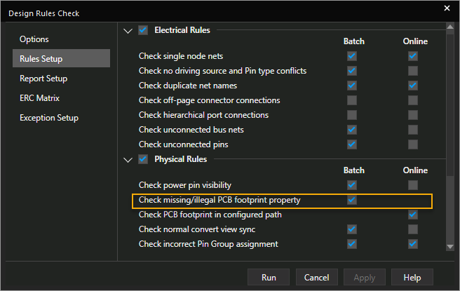
- Click Apply.
- Close the dialog box.
If required, you can also include the footprint information for the parts in the Bill of Materials (BOM) generated for your design. To generate a custom BOM with footprint information, perform the following tasks:
- In the project manager tab, select the design file.
- Select Tools – Bill of Materials.
The Bill of Materials dialog box opens.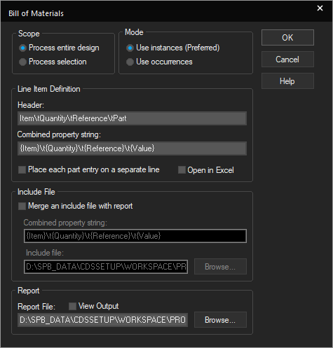
- Modify the following two default entries in the Line Item Definition section.
- In the Header text box, append
\tFootprints. - In the Combined property string text box, append
\t{PCB footprint}.
- In the Header text box, append
- Click OK to generate BOM.
The generated BOM has footprint information added in the last column.
Assigning Footprints to Components
While assigning a footprint to a schematic symbol, ensure that the number of pins in the schematic symbol match the number of the PCB footprint symbol, and the pin numbers in the schematic symbol match the pin numbers in the footprint.
To assigning footprint to one component using Property Editor, do the following steps:
- Right-click the required part in the schematic and choose Edit Properties to launch Property Editor.
- Specify the required value corresponding to the
PCB Footprintproperty.
To assign the same footprint to multiple components, do the following:
- Select the components.
- Right-click and choose Edit Properties to launch Property Editor.
- Right-click the
PCB Footprintrow (or column), and select Edit.
The Edit Property Values dialog box opens. - Specify the required value.
- Click OK.
To create a board in PCB Layout Expert (classic PCB editor) or OrCAD X PCB Layout (new user interface), you need to assign a valid PCB Footprint property for each part in the design. This includes all the mechanical parts in your design, although, in this case, you can use a dummy value for the PCB Footprint property. While designing a board using the schematic-layout flow, combined property strings can be used to pass user-defined properties as PCB Footprint property for PCB Netlist generation. This gives you the flexibility of defining a user-defined PCB Footprint property specifically for the Capture-PCB Layout Expert (classic PCB editor) and Capture-OrCAD X PCB Layout (new user interface) flows. As a result, you can define different PCB Footprint properties for different PCB flows.
CLASS with its value as MECHANICAL to the part, that is CLASS = MECHANICAL, with an appropriate PCB footprint.Specifying Alternative Footprints
You can specify alternative footprints using one of the following two methods:
- Using the
ALT_SYMBOLSproperty - Using the
FPLISTproperty
Using ALT_SYMBOLS Property
While specifying component footprint, the ALT_SYMBOLS property can be used to specify a list of alternative footprint names that can be used to substitute the primary footprint during interactive placement in PCB Layout Expert (classic PCB editor) or
OrCAD X PCB Layout (new user interface). The ALT_SYMBOLS property can be assigned to a package or to a component either at the library level or at the instance level.
The syntax of the ALT_SYMBOLS is:ALT_SYMBOLS '(Subclass:Symbol,...;Subclass:Symbol,...)'
Where:
Subclasscan either be TOP (or T) for top layer, or BOTTOM (or B) for bottom layerSymbolis the standard footprint name
For example, you can assign the ALT_SYMBOLS value: T:dip14_3; B:dip14_3 to the component, 7400.
To use the ALT_SYMBOLS property to specify a list of alternative footprints, do the following:
- Add the
ALT_SYMBOLSproperty to the component on which you want multiple footprint values. - Add the footprint information in the property value according to the syntax.
- Update the
allegro.cfgfile with the following information under the section,[ComponentDefinitionProps]:ALT_SYMBOLS = YES
Using FPLIST Property
The FPLIST property can also be used to specify a list of alternative footprints in Capture. This list substitutes the primary footprint during interactive placement in the layout editor. The FPLIST property can be assigned to a package or to a component either at the library level or at the instance level.
To use the FPLIST property to specify a list of alternative footprints, do the following:
- Add the
FPLISTproperty to the component on which you want multiple footprint values. - Add the footprint information in the property value.
You can separate the footprints by commas or use the syntax explained in the previous procedure, Using ALT_SYMBOLS Property. -
Update the
allegro.cfgfile with the following information under the section,[ComponentDefinitionProps]to map theFPLISTproperty to theALT_SYMBOLSproperty.FPLIST = ALT_SYMBOLSBefore addingFPLIST = ALT_SYMBOLS, ensure thatALT_SYMBOLS = YESis specified in theallegro.cfgfile.
Viewing Footprints
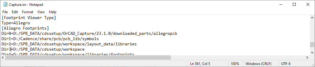
The footprint location in the installation is used to configure the Capture.ini file to ensure that it has a section on Allegro Footprints. The variables in this section define the directory locations for the .psm and .pad files. The relevant section of capture.ini is shown in the following example.

If you are using the custom footprints, Capture.ini must be updated such that Dir0, Dir1, Dir2,... variables point to the folder containing the footprints. This section of the capture.ini file is read by Footprint Viewer to display component footprint in Capture.
While working in Capture, you can view the footprints associated with the part in the Footprint Viewer window. This window provides a two-dimensional view of the footprint symbol of a selected part on the schematic. Along with the footprint symbol, it also shows pin numbers and pin names. The Footprint Viewer window is available from within the schematic. To view the footprint:
- Right-click the part.
- Choose Show Footprint.
 The Footprint Viewer window opens with the two dimensional view of the footprint corresponding to the selected part.
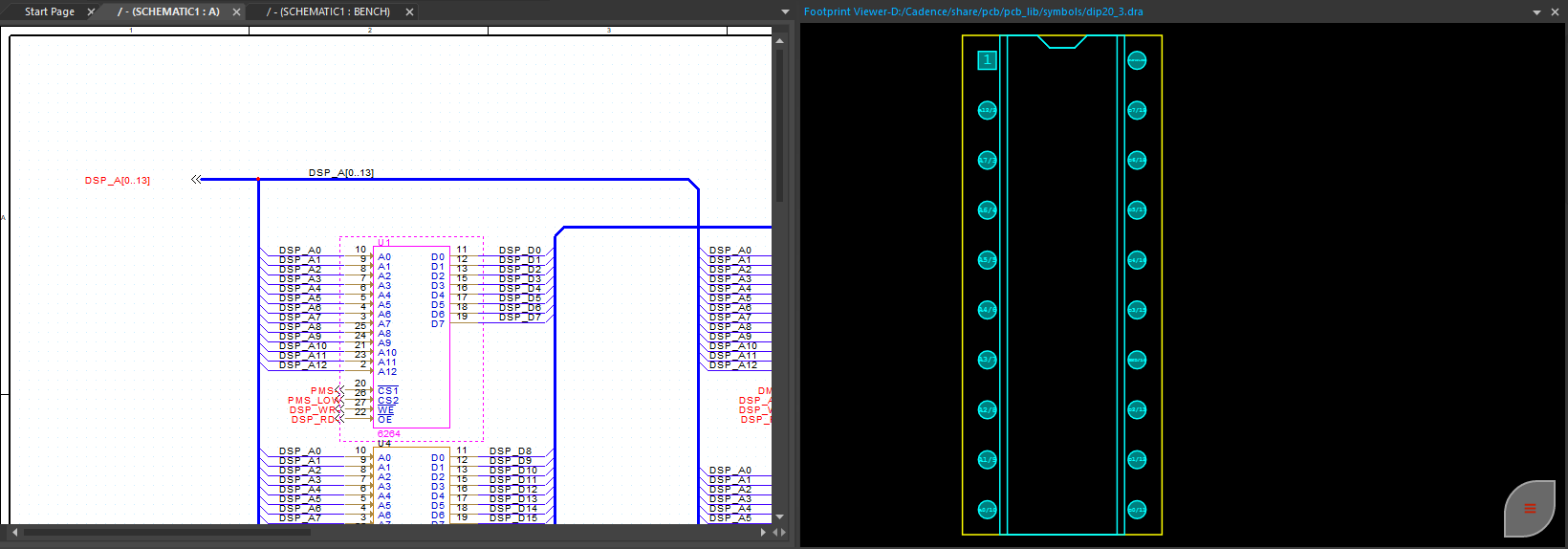
The Footprint Viewer window can be used to display footprint and pin information. To view the details of the footprint, click the footprint viewer menu ( ![]() ). The menu expands and shows various icons.
). The menu expands and shows various icons.
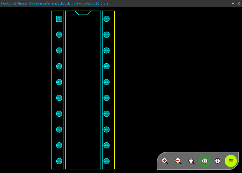
Each icon performs a specific function as explained in the following table:
| Icons in the Footprint Viewer menu | Click this icon to... |
|---|---|
 |
View or hide information about the footprint. The details are displayed at the top of the viewer. |
 |
View or hide information about pins. |
 |
The zoom scale is adjusted to fit the footprint in the footprint viewer window. |
 |
The current zoom scale is divided by the zoom factor to reduce the size of the footprint view. |
 |
The current zoom scale is multiplied by the zoom factor to magnify the footprint view. |
Mapping Symbol Pins with Footprint Pins
Footprint Viewer also supports cross-probing between the schematic design and the footprint view. When you select a symbol pin on the part, the corresponding pin along with pin details are highlighted in the footprint viewer.
Troubleshooting Footprint Viewing Errors
Problem: Footprints not displaying in the footprint viewer.
Solution: When viewing a footprint of a part, the footprint viewer selects the footprint to be displayed in the following order of preference:
- PCB Footprint property defined on the part instance.
- PCB Footprint property defined in the package properties of the part.
If none of the above properties or values are found, the viewer displays a blank canvas with an error. See the Session Log window for the list of errors.
- ERROR(ORCAP-1732): Could not retrieve PCB Footprint property. Unable to show footprint in viewer.
Ensure that for the selected component, a valid footprint value is defined for the PCB Footprint property.
- ERROR(ORCAP-1731): Allegro Footprints section could not be located in Capture.ini. Unable to show footprint %s in viewer.
Check the Capture.ini file to ensure that it has a section named [Allegro Footprints]. The variables in this section define the directory locations for the .psm and .pad files. These files are used by the viewer to display the footprint and pin information, respectively, in the viewer. The relevant section of the Capture.ini file is shown in the following figure:
For details on creating and editing the variables (including the Allegro Footprint variables) in Capture.ini, see Capture.ini Variables.
Instance-Level Properties for Physical Design
Besides the footprint property, there are other instance-level properties that can be defined on schematic components but are used during physical design. This section talks about some of these properties. Unlike footprint property, which is a must for board created, using the properties covered in this section is optional.
ROOM Property
The ROOM property is a component instance property that is used to group a set of components on the PCB board. For example, to ensure that a set of components are placed together in a particular section of the PCB board, add ROOM property on the schematic components and also define a room in the layot editor, components with same value of the ROOM property are placed in the defined area in the physical board design.
In Capture, use Property Editor to specify a value for the ROOM property on the schematic component.
Defining Properties on Nets
While designing a schematic in Capture, you can specify high-speed constraints as net properties and take them through a complete front-to-back flow. As net properties are passed to the physical netlist generated by Capture, these constraints are also passed to the layout editors. In the layout editor, you can modify these constraints by launching Constraint Manager. The following figure shows the flow of signal properties.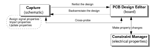
To view the list of high speed signal properties supported by Capture, open the Property Editor window, and from the Filter by: drop-down list, select Capture PCB Editor SignalFlow.
The properties are listed in the Flat Nets tab.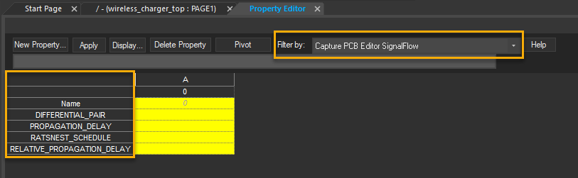 Use the Schematic Nets tab to display the net properties on the schematic. Adding or modifying high-speed signal properties is supported using the Flat nets tab of the Property Editor.
Signal Property Flow
This section lists the top-level design tasks to be performed for a design that has high-speed signal properties defined as net properties.
- Create a schematic.
- Select the net on which high-speed signal properties are to be assigned.
- Assign one or more of the following signal properties.
- DIFFERENTIAL_PAIR- PROPAGATION_DELAY- RATSNEST_SCHEDULE- RELATIVE_PROPAGATION_DELAY - Choose the PCB – Design Rules Check men command to perform design rule checks on the design.
- Choose the Tools – Create Netlist menu command to netlist the design.
- Right-click the board file name in the project manager window and choose Launch PCB Editor.
- In the layout editor—PCB Layout Expert (classic PCB editor) or OrCAD X PCB Layout (new user interface)—launch Constraint Manager.
- Open the board file in the PCB Editor.
- Click Setup – Constraint to open the Constraint Manager.
- Expand the Routing spreadsheet.
- Select the Min/Max Propagation Delays tab to view the
PROPAGATION_DELAYproperty or the Relative Propagation delay tab to view theRELATIVE_PROPAGATION_DELAYproperty. - Select the Wiring tab to view the
RATSNEST_SCHEDULEproperty.
This property appears in the Schedule column in the Topology section.
- Backannotate property changes.
If you make any signal property changes in Constraint Manager, you need to backannotate those changes to Capture.
- Open the board file in the PCB Editor and open the Constraint Manager.
- Make the desired property changes in Constraint Manager.
- In Capture, select Tools – Back Annotate.
The Backannotate dialog box appears. - Select the PCB Editor tab, set different backannotation options and click OK.
The Progress window reports the details of backannotation.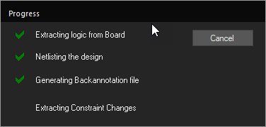
- Open the Property Editor window and verify any changes.
Limitations
The signal property flow has the following limitations:
- You cannot define extended nets.
- You cannot use multi match group power.
Adding PROPAGATION_DELAY Property
This property defines the minimum and maximum propagation delay constraint between any pair of pins in a net. By assigning this property to nets, you can make the router restrict the length of interconnect to meet timing margin. This property often is best applied to a common clock sourced designed bus.
To edit or specify the propagation delay on a net, do the following:
- Open the Property Editor window and select the filter to display the signal flow properties.
- Select the Flat Nets tab, and perform the following steps.
- Select the grid corresponding to the
PROPAGATION_DELAYproperty. -
Choose the Edit – Invoke UI or press the
CTRL+ushortcut keys.
The Propagation Delay dialog box appears.Alternatively, you can right-click on the grid corresponding to the
PROPAGATION_DELAYproperty and from the shortcut menu, select the Invoke UI command. - To specify the pin-pair, select one of the following options in the Pin Pair field.
- Longest/Shortest pin-pair(L:S)--To apply minimum delay to the shortest pin-pair and maximum delay to the longest pin-pair.
- Longest/Shortest Driver/Receiver(D:R)--To apply minimum delay to the shortest driver/receiver pin-pair and maximum delay to the longest driver/receiver pin-pair.
- All Drivers/All Receivers(AD:AR)--To apply Min/Max constraints to all driver/receiver pin-pairs.
- To create a new pin-pair, click the Add Pin Pair () button or press the
ALT+Ashortcut keys.
The Create Pin Pairs dialog box appears. Select the first pin for the pin-pair, then select the second pin, and click OK.
A pin-pair is created. The new pin-pair appears as a row in the Propagation Delay dialog box. You can define constraints for it
You can use the following methods to select multiple consecutive pins in the Create Pin Pairs dialog box:
- Using
Shift+DownArrow keys - Using
Shift+Leftmouse button click - Dragging the mouse pointer diagonally across the pins appearing in the combo box to select them
Similarly, you can use the CTRL+ click to select multiple nonconsecutive pins in the Create Pin Pairs dialog box.
- Using
- Enter a value specifying the minimum allowable propagation delay/length for the pin-pairs in the Min field.
- To specify the unit for minimum constraint, select one of the following options in the Min Rule field:
DELAYinns%MANHATANLENGTHin mills (mils), micron (um), millimeter (mm), centimeter (cm), and inches (in)
- Enter a value specifying the maximum allowable propagation delay/length for the pin-pairs in the Max field.
- Specify the unit for the maximum constraint by selecting unit value in the Max Rule field.
- Click OK in the Propagation Delay dialog box.
ThePROPAGATION_DELAYproperty is seeded in thePROPAGATION_DELAYgrid for the corresponding column. - Click the Apply button in the Property Editor to apply the
PROPAGATION_DELAYproperty on the nets. Moreover, if you have manually entered thePROPAGATION_DELAYsyntax, then Capture performs syntax validation and appends any syntax violations to the Session Log.
To delete an existing pin-pair, select the left-most cell of the pin-pair row and click the Delete Pin Pair () button or press the ALT+D shortcut keys.
You can assign the PROPAGATION_DELAY property to all the bits of a bus at the same time in the User Properties dialog box. Ensure that you use the correct syntax for specifying a value for the PROPAGATION_DELAY property. The syntax is:
<Pin_pair>:<min_value>:<max_value>
The pin-pairs can only be:
- L:S
- D:R
- AD:AR
You can also manually enter values in the grids corresponding to the PROPAGATION_DELAY property. After you enter a value in the PROPAGATION_DELAY property grid and click the Apply button, Capture performs syntax validation and if there is a syntax violation, the property is not applied and the details of the violation are appended to the Session Log.
You can populate multiple consecutive or nonconsecutive grids of the PROPAGATION_DELAY property at the same time. To do this, select the grids you want to populate and press the CTRL+E shortcut keys. The Edit Property Values dialog box appears. Specify the value that you want to be populated across all the selected grids in the dialog box. You can also use the shortcut keys CTRL+C and CTRL+V to perform standard copy/paste operations in the PROPAGATION_DELAY property grids.
Adding RATSNEST_SCHEDULE Property
This property specifies the type of ratsnest calculation that Constraint Manager performs on the net.
By using the RATSNEST_SCHEDULE property, you can meet a balance between time margin and noise margin. Based on your design need, you can define the configuration as MIN_TREE, MIN_DAISY_CHAIN, SOURCE_LOAD_DAISY_CHAIN, FAR_END_CLUSTER or STAR. This property useful in defining the placement of receiver or driver in multi-drop buses and asynchronous signals.
To specify the RATSNEST_SCHEDULE property:
- Select the grid corresponding to the
RATSNEST_SCHEDULEproperty. - From the drop-down list, select any of the following values:
- MIN_TREE – Indicates that the net rat should be displayed with the minimum spanning tree algorithm. Selecting this option can lead to formation of Ts at pins.
- MIN_DAISY_CHAIN – Indicates that a minimum length daisy-chain schedule is formed.
- SOURCE_LOAD_DAISY_CHAIN – Indicates that a source-to-load ECL daisy-chain schedule is used.
- FAR_END_CLUSTER – Automatically places a single Tpoint in a schedule at a calculated location.
- STAR – Specifies a ratsnest similar to FAR_END_CLUSTER without the Tpoint added.
Adding RELATIVE_PROPAGATION_DELAY Property
This property is an electrical constraint attached to pin-pairs on a net. It specifies a group of pin-pairs that are required to have interconnect propagation delays matching a specified delta (offset) and tolerance with respect to the target pin pair. A RELATIVE_PROPAGATION_DELAY group has a pin-pair against which all other pin-pairs in the group are compared. You can apply the RELATIVE_PROPAGATION_DELAY property to a source synchronous bus design, such as DDR interfaces.
To specify RELATIVE_PROPAGATION_DELAY property on a net, perform the following steps.
- In the Flat Nets tab of the Property Editor, select the grid corresponding to the
RELATIVE_PROPAGATION_DELAYproperty. -
Choose the Edit – Invoke UI menu command.
The Relative Propagation Delay dialog box appears.Alternatively, you can right-click on the grid corresponding to theRELATIVE_PROPAGATION_DELAYproperty and select the Invoke UI command from the pop-up menu or press theCtrl+Ushortcut keys. - To specify the pin-pair, select one of the following options in the Pin Pair field.
- Longest/Shortest pin-pair – To apply minimum delay to the shortest pin-pair and maximum delay to the longest pin-pair.
- Longest/Shortest Driver/Receiver – To apply minimum delay to the shortest driver/receiver pin-pair and maximum delay to the longest driver/receiver pin-pair.
- All Drivers/All Receivers – To apply Min/Max constraints to all driver/receiver pin-pairs.
- Select the scope as global or local. Select the scope as global to define the
RELATIVE_PROPAGATION_DELAYproperty between different nets of same match group. Select the scope as local to define theRELATIVE_PROPAGATION_DELAYproperty between different pin-pairs of same net. - Enter the relative value from the target net that all nets in the group should match in the Delta field.
- To specify the unit for delta, select Delay in ns or Length in mills (mils), micron (um), millimeter (mm), centimeter (cm), and inches (in) in the Delta Units field.
- Enter a value that specifies the maximum allowable propagation delay/length for the pin-pairs in the Tolerance field.
- To specify the unit for Tolerance, select one of the following options in the Tol. Units field:
- %
- DELAY (ns)
- LENGTH (mils, mm, cm, in)
- To create a new pin-pair, click the Add Pin Pair () button or press the ALT+A shortcut keys.
The Create Pin Pairs dialog box appears. - Select the first pin for the pin-pair, then select the second pin, and click OK.
A pin-pair is created. The new pin-pair appears as a row in the Propagation Delay dialog box. You can define constraints for it.
You can use the following methods to select multiple consecutive pins in the Create Pin Pairs dialog box:
- Using
Shift+Down Arrow keys - Using
Shift+click - Dragging the mouse pointer diagonally across the pins appearing in the combo box to select them
Ctrl+click to select multiple nonconsecutive pins in the Create Pin Pairs dialog box. - Using
- To delete an existing pin-pair, select the pin-pair row by clicking its left-most cell, and click the Delete Pin Pair () button or press the ALT+D shortcut keys.
- To set a pin-pair as the target net, select the pin-pair row and click the Set Target () button or press the ALT+S shortcut keys.
Target Pin Pair name is displayed and the Delta and Tolerance fields for the target pin-pair is set to'0'. - To delete the target status from a pin-pair, select the pin-pair row and click the Delete Target () button or press the ALT+T shortcut keys.
- To change the match group:
- Select a group from the list box.
- Type a new match group name.
Based on the match group selected, all nets contained in it will display in the Nets Attached box. - Click OK in the Relative Propagation Delay dialog box. The
RELATIVE_PROPAGATION_DELAYproperty is seeded in theRELATIVE_PROPAGATION_DELAYgrid for the corresponding column. - Click the Apply button in the Property Editor to apply the
RELATIVE_PROPAGATION_DELAYproperty on the nets. Moreover, if you have manually entered theRELATIVE_PROPAGATION_DELAYsyntax, then Capture performs syntax validation and appends any syntax violations to the Session Log.
You can use the User Properties dialog box to assign the RELATIVE_PROPAGATION_DELAY property to all the bits of a bus at the same time. Make sure that you use the correct syntax for specifying a value for the RELATIVE_PROPAGATION_DELAY property. The syntax is:
For the target pin-pair:
<match_group>:<scope>:<pin-pair>::
where <pin-pair> has the following syntax:
<pin1>:<pin2>
valid values of <scope> are L for local and G for global.
For non-target pin-pairs:
<match_group>:<scope>:<pin-pair>:<delta>:<tolerance>
The pin-pairs can only be:
AD:ARL:SD:R
You can also manually enter values in the grids corresponding to the RELATIVE_PROPAGATION_DELAY property, and click Apply. When you select the Apply button, Capture performs syntax validation and if there is a syntax violation, the property is not applied and the details of the violation are appended to the Session Log.
You can use the shortcut keys CTRL+C and CTRL+V to perform standard copy/paste operations in the RELATIVE_PROPAGATION_DELAY property grids.
RELATIVE_PROPAGATION_DELAY property at the same time. To do this, select the grids you want to populate and press the CTRL+E shortcut keys. The Edit Property Values dialog box appears. Specify the value that you want to be populated across all the selected grids in the dialog box.Adding DIFFERENTIAL_PAIR Property
This property represents a pair of flat nets that will be routed in a way that the signals passing through them are opposite in sign with respect to the same reference. This ensures that any electromagnetic noise in the circuit is cancelled out.
Creating Differential Pairs using Property Editor
To specify the DIFFERENTIAL_PAIR property for flat nets:
- Right-click the design in the project manager and choose Edit Object Properties.
The Property Editor window appears. - Click the Flat Nets tab at the bottom in the Property Editor window.
- Select the first flat net for which you want to create a differential pair.
- Select the grid corresponding to the
DIFFERENTIAL_PAIRproperty and specify a name for the differential pair. - Select the second flat net for which you want to create a differential pair.
- Specify the same differential pair name you specified for the first net.
- Click the Apply button. A differential pair between both the nets is created.
In addition to creating a differential pair using the DIFFERENTIAL_PAIR property in the property editor, you can use the Create Differential Pair command to create a differential pair between two flat nets in your design.
Editing Differential Pair
To edit or delete a differential pair from your design, do the following:
- In the project manager, click the design file (.dsn) or a schematic page file.
- Choose Tools – Create Differential Pair.
The Create Differential Pair dialog box dialog box opens. -
Ensure that the Net option is selected from the drop-down list.
All the flat nets in the design are listed in All Nets column in a sorted order. All net names starting with a numeric character are displayed first followed by all net names starting with an alphabet..To view nets of a particular type, specify the initial letters of the net in the Filter text box. All the nets of that particular type will appear in the All Nets column. For example, if you want to view all nets starting with the letter "A", then enter "A" in the Filter text box. All the nets starting with letter "A" will appear in the All Nets column. - Select a net from the All Nets column and click the button or double-click the net. The selected net appears in the Selections column.
- Repeat step 4 for the second net to be included in the differential pair.
To remove a net from the Selections column, double-click on the net name or select a net and click the button.
Once two nets are available in the Selections list-box, the Create button is enabled. - Specify a name for the differential pair in the Diff Pair Name text box.
-
Click the Create button. The differential pair is created between the selected nets. The differential pair name appears in the Selections column adjacent to the net name.
If the selected nets are not of the same type (for example, a power net and a non-power net) or they differ in the total number of pins in each selected net, then a message appears asking you to confirm the creation of a differential pair between the selected nets. - Click the Close button to close the Create Differential Pair dialog box.
Managing DIFFERENTIAL PAIR Property
The DIFFERENTIAL_PAIR property column is automatically updated with the differential pairs you create using the Create Differential Pair dialog box.
An Auto Differential pair can also be created for a bus. To do so, you need to put n & p as prefix and the Auto command creates differential pairs for all bits in the bus.
Viewing Differential Pair
To view a differential pair, do the following:
-
In the Create Differential Pair dialog box, select the Differential Pair option from the drop-down list.
All the differential pairs you created in your design appear in Diff Pairs column.To view differential pairs of a particular type, specify the initial letters of the differential pairs in the Filter text box. All the differential pairs of that particular type will appear in the Diff Pairs column. For example, if you want to view all differential pairs starting with the letter "DP", then enter "DP" in the Filter text box. All the differential pairs starting with letter "DP" will appear in the Diff Pairs column. -
Select a differential pair from the Diff Pairs column and click the (>) button or double-click the differential pair. The Selections column will display the name of the two nets associated with the selected differential pair.
You can use theCTRLorSHIFTkeys to move multiple differential pairs to the Selections column and view the nets associated with the selected differential pairs. - Click the Close button.
Modifying Differential Pair
To modify a differential pair, do the following:
- In the Create Differential Pair dialog box, select the Differential Pair option from the drop-down list.
All the differential pairs you created in your design appear in Diff Pairs column. -
Select the differential pair you want to modify from the Diff Pairs column and click the ( > ) button or double-click the differential pair. The selected differential pair along with the associated nets appears in the Selections column.
In case, you select a wrong differential pair for modification and want to revert back, double-click the differential pair in the Selections column. The differential pair is removed from the Selections column, but is available in your design. - Specify a new name for the differential pair in the Diff Pair Name text box.
- Click the Modify button. The new differential pair name is assigned to the selected nets.
- Click the Close button.
Deleting Differential Pair
To delete a differential pair, do the following:
- In the Create Differential Pair dialog box , select the Differential Pair option from the drop-down list. All the differential pairs you created in your design appear in Diff Pairs column.
-
Select the differential pair you want to delete from the Diff Pairs grid and click the ( > ) button. The selected differential pair along with the associated nets appear in the Selections column.
If you accidentally selected the wrong differential pair for deletion and want to revert back, double-click the nets in the Selections column. The differential pair is removed from the Selections column, but is available in your design. -
Click the Delete button. The differential pair set on the selected nets is deleted.
When you click the Delete button, the differential pair is deleted from the Selections column and the Diff Pairs column. - Click the Close button.
Creating Differential Pairs between Multiple Pairs of Flat Nets Simultaneously
Instead of creating differential pairs between two nets individually, you can quickly create differential pair between multiple pairs of flat nets simultaneously.
To create multiple differential pairs simultaneously, do the following:
-
In the Create Differential Pair dialog box, click the Auto Setup button.
The Create Differential Pair dialog box appears displaying all the flats nets and the corresponding differential pairs in the All Nets column.To view nets of a particular type, specify the initial letters of the net in the Filter text box. All the nets of that particular type will appear in the All Nets column. For example, if you want to view all nets starting with the letter "A", then enter "A" in the Filter text box. All the nets starting with letter "A" will appear in the All Nets column. - Specify a string (numeric or alphabet) that you want to precede the differential pair name. For example, if you specify "A" in the Prefix text box, then all the differential pair names that will be created will be preceded with "A".
- Specify the last digit of the first net name in the + Filter text box. For example, all net names ending with 1.
- Specify the last digit of the second net name in the - Filter text box. For example, all net names ending with 4.
- Click anywhere inside the Differential Pair Automatic Setup dialog box.
Capture displays a list of all differential pairs that can be created between all the nets that qualify the criteria set in the + Filter and - Filter text boxes. Also, the Differential Pair Name is preceded with the prefix specified in the Prefix text box.
The +Net and -Net grid displays the two nets associated with a differential pair.
If you do not want a specific differential pair to be created, select the row containing the differential pair and click the Remove button or double-click the row containing the differential pair. The selected row disappears.If the nets forming a differential pair are of the type DP+ and DP-, the name of the differential pair is set to DP. For other pairs of nets, the name of the differential pair is of the type DP. - Click the Create button.
All the differential pairs displayed in the Selections column are created. - Click the Close button to close the Differential Pair Automatic Setup dialog box and go back to the Create Differential Pair dialog box.
VOLTAGE Property
In addition to the High-Speed signal properties, another commonly used property assigned on a design net is the VOLTAGE property.
When assigned on a part as an instance-level property, is not transferred to the PCB Editor netlist. Only when the VOLTAGE property is applied to a flat net, it is passed to PCB Editor netlist as an electrical constraint.
The Voltage property only takes a numeric value. For example, if you specify the value as 10mV, the non-numeric part is ignored. By default, the property value is measured in volts. To specify the value of the VOLTAGE property as 3mV, specify the value as 0.003 and not 3mV.
Properties on Power Pins
While preparing your design for physical layout, it is important that the power pins in your design are handled properly, because depending on the part type, power pins may be shared across a package.
This section details properties related to POWER PINS that can be used in the Capture – PCB Editor design flow to ensure that the design is successfully netlisted.
POWER_PINS property
Power pins are usually defined when you generate a part using Part Editor. For example, during part generation you can define the pins 1, 3, and 7 as VCC pins; and 2, 4, 5, and 6 as GND. However, after you have instantiated a part in the schematic, if required, you can use override the part-level assignments by using the POWER_PINS property.
To use the POWER_PINS property
- Launch Property Editor on the selected part.
- Click New Row.
- In the Add New Row dialog, enter the property name as POWER_PINS.
- In the Value text box, type the power pins assignments. The syntax to be followed is:
<pin_type>:<comma seperated list of pinnumbers>; <pin_type>:<list of pinnumbers>
Example1:
To assign the pins 4, 5, and 7 to the VCC net, the value assigned to the POWER_PINS property should be (VCC:4,5,7)
Example2:
To assign the pins 4, 5 and 7 to the VCC net, and the pins 16, 18, 21 to the GND net, the power pins assignment is defined as (VCC:4,5,7;GND:16,18,21)
The power pin assignments that you perform through the POWER_PINS property are defined at the schematic level, and the changes are not reflected on the part. As a result, on opening the selected part in the Part Editor, the modified pin assignments are not reflected. However, in the Capture - PCB Editor flow, the POWER_PINS property on the part takes precedence over the part instance pin assignments.
Assigning Power Nets to Invisible Power Pins
It is a common practice to create parts with invisible power pins. When these parts are instantiated in schematic, Capture connects invisible power pins to a default power net that shares a name with the pin. For example, if pin number 14 and 28 are marked as VCC pins, these are by default connected to the global VCC net in the design.
Capture provides you a mechanism to override this default behavior and assign different values to different power pins. You can achieve this using one of the following methods.
- Using Assign Power Pins command
- Using the POWER_GROUP property
Using Assign Power Pins command
The Assign Power Pins command can be used on a component or on a design to view the invisible power pins of a single component or of all components in the designs.
- Select the component instance or the root design.
- From the Tools menu, choose Assign Power Pins.
The Assign Power Pins dialog box displays.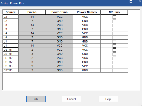 The Power Names column lists the power net connected to the power pin by default.
 - To connect the power pin to a different power net, click on the Power Names grid.
- From the drop-down list, select the power net to be associated with the power pin.
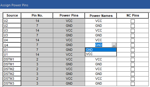
- Make changes for all the required power pins and click OK.
If you now save the design and launch Property Editor, the new value is assigned to the POWER_GROUP property on the component.
Using the POWER_GROUP property
This section discusses how to use the POWER_GROUP property to change the default power net associated with an invisible power pin of a component. This is a component definition property that circumvents the need to edit the pin properties for each invisible power pin on a particular component. Using this property, you can assign different values for the power net used on a particular design, instance or occurrence.
POWER_GROUP can be assigned with a unique value for multiple occurrences in the design. Multiple occurrences of a part can have different values for the POWER_GROUP property, allowing you to control power net connections at the occurrence level.
With the POWER_GROUP property added to parts with invisible power pin(s), you can overwrite power pins with the new power pin name at the instance level. If this property is used, POWER_GROUP is added to your combined property string so that you can annotate correctly.
The POWER_PINS property determines the power net in your design, to which invisible pins are connected. In order to connect multiple (invisible) power pins to the same net, you assign the POWER_GROUP property to each component that includes these pins.
To avoid using visible power pins in the Capture-PCB Editor flow
- Create a part with invisible power pins.
- Place the part in your design. By default, Capture connects any power pins on the part to the corresponding global nets. So, for example, if the part included (invisible) power pins VCC, VDD, GND, and AGND, each of these would be connected to a corresponding global net of the same name.
- In order to change the default power connections, select the part and add the POWER_GROUP property to reassign the connections for any of the power pins. So, for example, to change the connection for VDD to VCC, you would add the POWER_GROUP property as follows:
POWER_GROUP VDD=VCC
(To change the value of this property, open the Property spreadsheet, then go to the Capture-PCB Editor Property filter and enter "VCC=VDD" as the value of the POWER_GROUP property).
In this example, pins in the netlist that would have been assigned to the VDD net are instead assigned to VCC and the netlister correctly reflects this change into the netlist.
POWER_GROUP : VCC=AVPP; GND=HGNDPOWER_GROUP : AGND=GNDReassigning power pin connections
When reassigning nets, Capture uses precedence rules for the POWER_GROUPS property in the same way they are used for other component definition properties. Therefore, when a higher level property value overrides property values at a lower level, even if there are multiple occurrences at the lower level, each of these occurrences is replaced by the higher-level properties.
For example, assume you have an instance with various power signals VCC, VDD, VPP, and VSS. If you want all these signals to be shorted to VCC, then assign the following POWER_GROUP property in the Attribute form of the Property Spreadsheet:POWER_GROUP = VDD=VCC;VPP=VCC;VSS=VCC
This results in the following assignments:
| On the part | On the schematic instance | In the PSTCHIPS.DAT file |
|---|---|---|
|
|
|
|
Assigning No Connect Pins in Capture-PCB Editor Flow
While designing a schematic, it is a good design practice to ensure that there are no unconnected pins in the schematic. To ensure that an unconnected pin in a schematic page, is by design and not an oversight, no connect (NC) symbols must be used. You should always connect a no connect symbol to open pins for better readability of the design. The Design Rules Check tool ignores unconnected pins with no connect symbols.
If a pin with a no connect symbol is connected to a net, the no connect symbol has no effect on the pin and becomes invisible. If the pin is later disconnected from the net, the no connect symbol becomes visible again.
Assigning No Connect Pins
To successfully create the physical layout of a schematic, in PCB Editor, you need to ensure that for all components, the number of pins in the schematic must equal the number of pins specified in the PCB Editor footprint.
When you generate the PCB Editor netlist for a Capture schematic, the information about the number of pins in a component is included in the PSTCHIP.DAT file. The total number of component pins includes regular pins, power pins, and NC (no-connect) pins if present.
If you have numbered through-hole pins or non-electrical pins on the board, do one of the following to the part in your design:
- Add the NC property to the part. For the value of the NC property, use the pin numbers of the non-electrical pins separated by commas.
For example, an 8-pin footprint with the two through-holes being pins 7 and 8, results in a 6-pin part on the design with an NC property containing the value of 7,8. - Place a No Connect symbol on pins that you do not want to be connected to anything:
- Launch Property Editor to display the component properties.
- In the Pins tab, select the Is No Connect check box for the pin to be marked as NC pin.
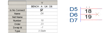
In the design, you will see an X symbol on the pin. So, for the previous example you would have an 8-pin part in your design with No Connect on pins 7 and 8.
- Do not connect any nets to the non-electrical pins on the part. So, in the earlier example, there is an 8-pin part with nothing connected on pins 7 and 8.
PSTXNET.DAT file, as nets with the name NC. Therefore, you should avoid the net alias NC in your design. The NC property discussed in the first option, above, appears in the PSTCHIP.DAT file in the NC_PINS line rather than being added to the NC net in PSTXNET.DAT or PSTXPRT.DAT. Therefore, all pins connected to the NC net are unconnected on the PCB.You have to account for unconnected pins of multi-section parts, such as mounting holes of multi-row connectors. To do so, however, you do not want to make the part heterogeneous with the mounting holes as pins on one section or distributed among the sections. Instead, make the part homogeneous and add the NC property to each section of the part, with the same pins listed for the NC property on all sections. In the part editor, you can add an NC property to each part in turn by choosing Previous Part from the View menu and placing the same NC property on all sections.
Assigning No Connect Power Pins
When you take your design to the board, by default, all powers pins will be shorted together (all VCC pins are shorted and all GND pins are shorted). This means that on your board you will need to route all the power pins. In the case of large pin devices (like FPGAs), this can be a tedious and time-consuming task.
To overcome this, you can select the power pins on your design that you want to route and then set all the other power pins as NC pins. This ensures that you then only need to route the power pins that are not set as NC pins.
Since a design may potentially have a large number of schematic folder and pages, Capture allows you to specify the NC pin command for power pins at multiple levels of the design. At the design level, you can view the list of the power pins in the entire design. You can also select and view the power pins at schematic folder level, schematic page level or even down to the level of one or more selected objects on a schematic page.
To specify a power pin as an NC pin, do the following:
- In the project manager, select the design, schematic folder, or schematic page that contains the power pins you need to set as NC.
Or
To specify a power pin as an NC pin at the object level in a schematic page, select an object on the schematic page. -
From the Tools menu choose Assign Power Pins to view the list of invisible power pins.
The Assign Power Pins dialog displays listing all the invisible power pins in the object (or objects) selected in the project manager.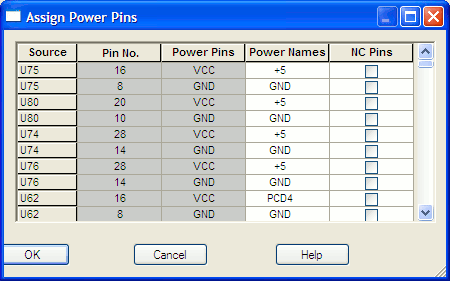 If the selected object contains no invisible power pins, a warning is displayed in the Session window.
 - To specify a power pin as a no connect pin, select the corresponding NC Pins check box.
On selecting the NC Pins check box, the corresponding Power Names field is disabled. The field lists the default Power net connected to the power pin. - Click OK to save your changes and to close the dialog box.
Property Flow from Schematic to Layout Editor
When you netlist a Capture schematic, not all properties defined in Capture are transferred to the layout. For a property to flow from Capture to the layout editor, it needs to be included in the configuration (.cfg) file.
The configuration file specifies net, part (function), and component instance and component definition properties. This mapping determines what properties may be netlisted from Capture to the layout editor or back annotated from the layout editor to Capture. If a Capture property is not included in the configuration file, it is not passed to the layout editor. Similarly, if a layout editor property is not listed in the file, it does not get back annotated to Capture.
Layout Editor Configuration File
The default configuration file installed with Capture is available at <installation_directory>\tools\capture\allegro.cfg. This file has a predefined set of default properties for components, functions, nets, and pins, listed under different sections of the configuration file. By default, allegro.cfg is divided into five sections, written in a Windows.INI format.
- ComponentDefinitionProps - The layout editor component definition properties, output in
PSTCHIP.DATfile - ComponentInstanceProps - The layout editor component instance properties, output in
PSTXPRT.DATfile - netprops - The layout editor net properties and all pin level properties, output in the
PSTXNET.DATfile - functionprops - The layout editor function properties, output in the
PSTXPRT.DATfile - pinprops - pin-level properties transferred between Capture and the layout editor
The following is a section of the default configuration file included in the Capture installation:
Section of allegro.cfg
[ComponentDefinitionProps]ALT_SYMBOLS=YESCLASS=YESPART_NUMBER=YESTOL=YESVALUE=YESPOWER_GROUP=YESSWAP_INFO=YESCDS_FSP_FPGA_SYMBOL=YESASI_MODEL=YES
[ComponentInstanceProps]GROUP=YESROOM=YESVOLTAGE=YESSIGNAL_MODEL=YESNO_XNET_CONNECTION=YES
[netprops]BUS_NAME=YESCLOCK_NET=YESDIFFERENTIAL_PAIR=YESDIFFP_2ND_LENGTH=YESDIFFP_LENGTH_TOL=YESECL=YESECL_TEMP=YESELECTRICAL_CONSTRAINT_SET=YESEMC_CRITICAL_NET=YESIMPEDANCE_RULE=YESMATCHED_DELAY=YESMAX_EXPOSED_LENGTH=YESMAX_FINAL_SETTLE=YESMAX_OVERSHOOT=YESMAX_VIA_COUNT=YESMIN_BOND_LENGTH=YES...
...
VOLTAGE_LAYER=YESCDS_FSP_NET=YESCDS_FSP_UID=YESCDS_FSP_BUS_INDEX=YESNET_GROUP_GRP_NAME=YES
[functionprops]GROUP=YESHARD_LOCATION=YESNO_SWAP_GATE=YESNO_SWAP_GATE_EXT=YESNO_SWAP_PIN=YESROOM=YESCDS_FSP_IS_FPGA=YESCDS_FSP_INSTANCE_ID=YESCDS_FSP_TERM_NAME=YESCDS_FSP_UID=YESCDS_FSP_TERM_TYPE=YESCDS_FSP_MAPPED_CELL=YESCDS_FSP_TERM_INDEX=YESCDS_FSP_FPGA_SYMBOL=YES
[pinprops]NO_DRC=YESNO_PIN_ESCAPE=YESNO_SHAPE_CONNECT=YESNO_SWAP_PIN=YESPIN_ESCAPE=YESPIN_SIGNAL_MODEL=YESNET_SHORT=YES
How properties are netlisted from Capture to PCB Editor
Not all properties in the configuration file show up as properties in PCB Editor. Some of these properties are used in generating portions of the netlist PST*.DAT files.
In PCB Editor, component properties (package properties in Capture) take precedence over function properties (part properties in Capture). So in the netlist, a package property value is used if both a part and package have values for the same property. Capture always uses the occurrence values in the netlist.
Package (component) properties, which are found in the PSTCHIP.DAT and PSTXPRT.DAT netlist files, can be viewed in PCB Editor using the Show Element command on a component. For example, PCB Editor has defined VALUE as a Component Definition property so it appears under this heading in the Show Element dialog box. Other properties such as CLASS or JEDEC_TYPE are also listed.
Part (function) properties are found in the PSTXNET.DAT file and can appear as Component Definition properties if they are predefined in PCB Editor and if you list them in the [ComponentDefinitionProps] section of the configuration file. Function properties are listed in the [functionprops] section of the configuration file.
Net properties appear in the PSTXNET.DAT/PSTXPRT.DAT file under the NET_NAME section.
For a design, you can have multiple configuration files. However, the configuration file to be used while generating PCB Editor netlist needs to be specified in the Setup dialog box launched from the PCB Editor tab of the Create Netlist dialog box.
User-Defined Properties in Capture - PCB Editor Flow
For a Capture design that has user-defined properties to be transferred to PCB Editor, you need to do the following:
- In Capture, add the property on the required design object.
- Modify the configuration file to include the name of the custom property in the appropriate section of the configuration file.
- While specifying the options for generating the PCB Editor netlist, in the Create Netlist dialog box, ensure the following.
- The file modified in step 2 is specified as the configuration file.
- The Allow User Defined Property option is selected.
If you now generate the PCB Editor netlist, the custom property is pushed to PCB Editor. The property is visible in PCB Editor. Any changes made to the property value in PCB Editor will be updated in the Capture schematic, when you run the back-to-front flow.
Guidelines for Updating Configuration File (allegro.cfg)
Following should be kept in mind while modifying a configuration file:
- User-defined property names are case sensitive. PCB Editor properties consist of all capitalized letters. If you have problems seeing properties netlisted or back annotated, check the spelling and the case of the property names.
The component definition propertiesVALUE, ALT _SYMBOL, JEDEC_TYPE, andCLASSare not back annotated as they cannot be changed in PCB Editor. - Do not use
NOafter the=sign for a property.
NO becomes the property alias. If you do not want a property to be passed, you must delete it from the configuration file. - Some properties listed in the configuration file are not applicable in all versions of PCB Editor. Including these properties in the configuration file is not a problem since they would not be used.
A list of typical properties used with PCB Editor may be found in the Capture PCB Editor filter of Property Editor.
This filter is built on thePREFPROP.TXTfile, which is copied to your Capture directory during installation.
Aliasing properties in configuration file
While migrating an old design to the latest version of the product, you may need to use aliases in the configuration file to map an old PCB Editor property to a new one. The following table lists some PCB Editor properties where aliasing is required:
Examples of Property Aliasing
|
Old property name |
New property name |
|
|
|
|
|
|
|
|
|
|
|
|
The TOPOLOGY_TEMPLATE_REVISION property is obsolete and therefore ignored. If you have a legacy PCB Editor design that uses DELAY_RULE, for example, you can change the line in the configuration file from:
PROPAGATION_DELAY=YES
toDELAY_RULE = PROPAGATION_DELAY
With an alias, you can have two different names for equivalent properties, one for Capture and one for PCB Editor. In the above example, DELAY_RULE properties get passed into the netlist as PROPAGATION_DELAY properties. You can include one of the above lines in the configuration file. Alternatively, you can modify your design to use PROPAGATION_DELAY rather than DELAY_RULE.
Creating PCB Editor Board
You can generate PCB Editor board by using the New Layout dialog box.
To generate PCB Editor board file, perform the following tasks:
- Select PCB – New Layout.
The New Layout dialog box opens.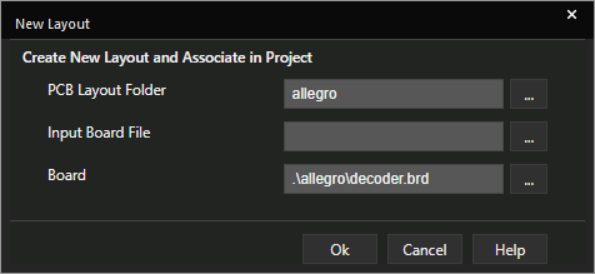
- The PCB Layout Folder text box shows the name of the folder in your design directory where the
*.BRDandPST*.DATfiles are to be saved. For a Constraint Manager-enabled design, the zip file,pstdedb.cdszis created instead of PST files.The default location is the directory named the last time this dialog box was invoked for the current design. If this is the first time the design is being netlisted, the default location will be an Allegro subfolder in your design directory. If the netlist files have been generated previously for the project, then the default is netlist directory of the board on which an operation was done the last time.
-
In the Input Board File text box, specify the name for an existing layout file to be used as template for generating the initial board file for the current design.
This field is optional if you are creating a new board. - In the Board text box, specify a name for the output board file to be generated.
If you want to update an existing board, this field should have the same value as specified in the Input Board File text box.
- To open the output board file immediately after the design is netlisted, ensure that the required layout tool is specified in the Design Sync Setup dialog box. The extension of the input and output board files specified in step 2 and step 3, respectively, is related to the layout tool selected in the Design Sync Setup dialog box.
The supported options are:
-
OrCAD X PCB Layout Expert (classic pcb editor): Generates the physical layout file with the
.brdextension and opens the board file in PCB Editor. - OrCAD X PCB Layout (new user interface): Generates the physical layout file with the
.brdextension and opens the board file in OrCAD X PCB Layout (new user interface). - Allegro X Advanced Package Designer: Generates the physical layout file with the
.mcmextension and opens it in Allegro X Advanced Package Designer. -
Update Layout and Do Not Open: Generates the board file in the path specified in step 3, but no application is launched.
-
- Click OK to close the New Layout dialog box and create and open the
.brdfile.
On successful netlisting, blank board file is opened in the selected layout editor. You can now place the parts and route your ratsnest.
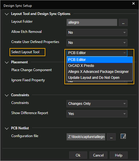
Setting up Advanced Options for PCB Flow
Use the Design Sync Setup dialog box to set up options related to the layout tool, PCB netlist, and the Update Layout and Update Schematic dialog box.
To set up these options, do the following:
- Choose the PCB – Design Sync Setup menu command. Alternatively, click
 in the Update Layout or Update Schematic dialog box.
The Design Sync Setup dialog box opens.
- Specify the required preferences.
For details about each option, see Design Sync Setup dialog box. - Click Ok.
Processing Changes after Board Creation (ECO)
You can view the differences with respect to the selected board, and synchronizes the layout from schematic using the Update Layout dialog box. It shows the type of change, addition, modification, or removal of a design object.
To review design connectivity changes in real-time and synchronize the layout from schematic, do the following tasks:
- Select PCB – Update Layout or click
 .
.
Alternatively, right-click the board file under the Layout folder of project manager, and select Update Layout.
The Schematic drop-down displays the location of the project file.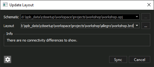
- The Layout drop-down list displays the location of the board file.
If there are multiple board files, click the drop-down list to select the required board file. - The Preview section displays the all the differences from Schematic to Layout:
- Change Type
This can include Gate Swap, Ref Des, Pin Swap, Component Property, Net Property, Pin Property, Component, Net, and Connection. - Object
- Action
- New Value
- Old Value
- Change Type
- Click the Sync button.
When you click this button, forward annotation of changes takes place from Capture to the layout editor—OrCAD X PCB Layout Expert (classic PCB editor) or OrCAD X PCB Layout (new user interface). The Constraint Difference Report is published.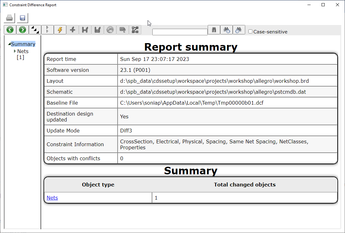
You can view the differences with respect to the selected schematic, and synchronizes the schematic from layout in the The Update Schematic dialog box.It shows the type of change, addition, modification or removal of a design object.
To review design connectivity changes in real-time and synchronize the schematic from layout, do the following tasks:
- Select PCB – Update Schematic or click
 .
.
Alternatively, right-click the board file under the Layout folder of project manager, and select Update Schematic. - The Schematic drop-down displays the location of the project file.
- The Layout drop-down list displays the location of the board file.
If there are multiple board files, click the drop-down list to select the required board file. - The Preview section displays the all the differences from layout to schematic:
- Change Type
This can include Gate Swap, Ref Des, Pin Swap, Component Property, Net Property, Pin Property, Component, Net, and Connection. - Object
- Action
- New Value
- Old Value
- Change Type
- Click the Sync button.
When you click this button, changes in the PCB Editor board are back annotated to the Capture schematic to ensure the physical board design is consistent with the logical schematic design.
Cross Probing for PCB Editor
After creating the board file, you place and route the board. This includes placing the parts in OrCAD X PCB Layout Expert (classic PCB editor) or OrCAD X PCB Layout (new user interface), Allegro X Advanced Package Designer and routing the nets. Sometimes, you may also require to swap pins or sections or functions to make routing easier. You can select the components from the Select elements for placement list in the Placement dialog box and then place them directly on the board. You can also place the components directly from the schematic design. This feature is called cross-probing. Between Capture and PCB Editor, there are two cross-probing functions: cross highlighting and cross-selection.
Cross-probing between PCB Editor and Capture uses Intertool Communication (ITC).
To enable ITC in Capture:
- Choose Options – Preferences.
- In the Preferences dialog box, select the Miscellaneous tab.
- Select the Enable Intertool Communication check box.
- Click OK.
When you export the netlist for your design into PCB Editor, cross-probing is enabled.
Both the backslash ( \ ) and underscore ( _ ) characters in net names interfere with cross-probing. Also, the design name must not contain period ( . ).
Cross Selecting between Capture and PCB Layout Expert (Classic PCB Editor)
If you are placing parts in PCB Editor using Place – Manually command, select one or more parts in Capture and the corresponding parts will be selected in the Placement dialog box in PCB Editor. This option is only available when PCB Editor is active (running) and Intertool Communication (ITC) is enabled in Capture.
- The cross probe function works only in the Interactive Place mode of PCB Editor.
- If you select a part/pin/signal in PCB Editor that has been deleted from Capture design, a warning message will be printed in the Session log of Capture.
Cross Highlighting between Capture and PCB Layout Expert (Classic PCB Editor)
Cross highlighting applies to three different types of objects: parts, nets and pins. Here are the general rules of cross-probing:
- If PCB Editor is in highlight mode, you can select an object in PCB Editor, and the corresponding logical element in Capture is highlighted.
- If PCB Editor is in dehighlight mode, when you dehighlight a physical object, the corresponding logical element is dehighlighted in Capture. Deselecting an element in Capture dehighlights the corresponding element in PCB Editor.
- In Capture, when you select a component, its corresponding physical part is only highlighted in PCB Editor if the PCB Editor highlight mode is active. Otherwise, selection in Capture has no effect in PCB Editor, unless you are using cross-selection.
The following tables show how highlighting and dehighlighting work between the two tools:
|
Selecting in Capture |
Result in PCB Editor |
|---|---|
|
Select a part |
Highlights the corresponding component |
|
Select a wire |
Highlights all trace segments in the net |
|
Select a pin |
Highlights the corresponding pad |
|
Deselecting in Capture |
Result in PCB Editor |
|---|---|
|
Deselect a part |
Dehighlights the corresponding component |
|
Deselect a wire |
Dehighlights all trace segments in the net |
|
Deselect a pin |
Dehighlights the corresponding pad |
|
Highlighting in PCB Editor |
Result in Capture |
|---|---|
|
Highlight a component |
Highlights all parts in the corresponding package |
|
Highlight a net |
Highlights the entire corresponding flat net |
|
Highlight a pad |
Highlights the corresponding pin |
|
Dehighlighting in PCB Editor |
Result in Capture |
|---|---|
|
Dehighlight a component |
Dehighlights all parts in the corresponding package |
|
Dehighlight a net |
Dehighlights the entire corresponding flat net |
|
Dehighlight a pad |
Dehighlights the corresponding pin |
Locking Components during Cross-Probing
When you cross-probe between Capture and PCB Editor, you need to keep selecting components in your design to place them on the board.
In many cases, you create elaborate designs with a large number of components and intricate connectivity. So when you keep selecting the components and nets on your design, you might inadvertently shift a component. This shift, in some cases, might even cause issues of connectivity.
To avoid shifting a component during cross-probing, you can temporarily lock the component. This ensures that the component is locked to the canvas and cannot be moved.
However, this is a temporary locking operation and the lock status of the object is lost as soon as you click anywhere on the page or on another object. To create a persistent lock on a component you need to use the Graphical Operation (GOp) Locking feature in Capture.
Pin Swapping In Capture-PCB Editor Flow
PCB Editor allows function/section swapping depending on the logical pin list on the function/section. This plays a key role when you create asymmetrical parts. If you have used invisible pins in a Capture design, these pins are not used by PCB Editor while deciding swappable sections. That is, body sections do not play any role in section swapping. PCB Editor calls each section as a function. A function is made with only logical pin list and any two functions that have same logical pin list are swappable in PCB Editor.
In the Capture-PCB Editor flow (only) you can perform pin swapping between parts in a heterogeneous package by using the SWAP_INFO or the SPLIT_INST property. This is useful when you are working with parts that have large pin counts (such as BGA parts). For information about the SWAP_INFO and the SPLIT_INST property, see Using the SWAP_INFO property and Using the SPLIT_INST property. You can assign the SWAP_INFO or the SPLIT_INST property to a part at the library level (recommended) or at the instance level.
If you want to do pin swaps in PCB Editor and then back annotate those changes, you must set up the pin properties in Capture first. Pin swap specifications will be produced only if the Swap Id properties are set correctly on pin-swappable parts.
To do this, you can open the part in the library or select the part of interest in your design. Then, from the Edit menu, choose the Part option. From the View menu, choose Package, then from the Edit menu, choose Properties.
In the Properties spreadsheet set the PinGroup value to 1 for each swappable (input) pin of the part. If you have a multi-section part you only have to set the PinGroup value for one section; the part editor adds the same value for all the other sections automatically. For example, on a 7400, set the PinGroup to 1 for pins 1 and 2. Leave the other PinGroup values blank and they are filled in automatically when you click the update all button. (PinGroup = 1 for pins 1, 2, 4, 5, 8, 9, 11, and 12.)
When you select a pin and edit its properties, the value shows as the Swap Id property. The default value is -1, meaning the pin is not swappable. Therefore you must add the PinGroup property to enable pin swapping for your part if you want to be able to swap pins. Swap Id value of 0 and greater than 0 in the property editor mean that the pin is swappable. To unswap a pin, you can delete the PinGroup property in the Property Editor window. You can see which pins are swappable in the PSTCHIP.DAT file by looking for the PIN_GROUP line under the pin name.
Using the SWAP_INFO property
To enable pin swaps across sections of heterogeneous split parts in PCB Editor, a SWAP_INFO property has been introduced in PCB Editor.
The SWAP_INFO property defines a logical group of parts of a package in a heterogeneous (split) part. This allows two pins - having the same PIN_GROUP property - to be swapped within a logical group, regardless of the physical availability of the pin in the given part of the package.
The SWAP_INFO property is defined under the [ComponentDefinitionProps] section in the allegro.cfg file. The swap information is written into body section of the primitive of the pstchip.dat file. PCB Editor reads the SWAP_INFO property and accordingly allows pin swaps across sections.
If you have a customized PCB Editor configuration file (allegro.cfg) for your Capture PCB Editor netlister, you need to add the following entry under the [ComponentDefinitionProps] section in the Allegro.cfg file:
[ComponentDefinitionProps]
SWAP_INFO=YES
Example
The usage of the SWAP_INFO property is described using a split part.
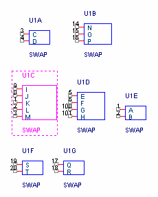 The above figure shows the example of a heterogeneous (split) part having seven parts-per-package. Let us assume that parts with the reference designators:
- U1A and U1B, form one logical section
- U1C, U1D and U1E, form the second logical section
- U1F and U1G, form the third logical section
In this scenario, the value of the SWAP_INFO property on all the parts of the package will be defined as:
(S1+S2),(S3+S4+S5),(S6+S7)
The logical section (S1+S2) indicates that a pin in section S1 is swappable with a pin in section S2, provided they have the same PIN_GROUP value. Therefore, pin 3 of S1 can be swapped with pin 14 of S2 if they have the same PIN_GROUP value.
In a SWAP_INFO syntax, the logical and physical sections are separated by a  sign.
sign.
Note the following when you use the SWAP_INFO property:
- You must assign the SWAP_INFO property to all parts in the heterogeneous package for which you want to perform pin swapping.
- There must not be any duplicate pins on any of the parts in the heterogeneous package if they are to receive the SWAP_INFO property.
- Ensure that you name the sections as (S1+S2+ S3+…Sn). If you use any other notation for naming the sections, the SWAP_INFO property will not work.
- Ensure that you use `(` and `)' brackets for defining single sections also. For example, If you have a split part having 6 sections (S1 to S6) and wish to add the SWAP_INFO property such that swapping happens only between sections S5 and S6. In that case you need to add the SWAP_INFO value as (S1), (S2), (S3), (S4), (S5+S6).
- The SWAP_INFO property does not function for homogeneous parts. No DRC errors will be reported if the SWAP_INFO property is assigned to a homogeneous part.
- DRC errors will not be reported if there are syntax or semantic errors in the value of the SWAP_INFO property.
Using the SPLIT_INST property
The SPLIT_INST property provides a method for swapping pins between parts of a heterogeneous package. You can assign it to a part in a library, or to an instance in a design.
When you assign the SPLIT_INST property to a part at the library or instance level, all lower level occurrences of that part (on the schematic) inherit the property.
The SPLIT_INST property has two possible values: TRUE and FALSE (default). Assigning a value of TRUE to the SPLIT_INST property on the parts of a heterogeneous package indicates that the netlister treats the package as a flat part, thus allowing pin swapping between the parts of that package.
When you use the SPLIT_INST property, be aware of the following points:
- You must assign the SPLIT_INST property to each part in the heterogeneous package for which you want to perform pin swapping.
- The SPLIT_INST property does not function for homogeneous parts (nor will the Design Rules Check tool detect an error if SPLIT_INST is assigned to a part that is part of a homogeneous package).
- There must not be any duplicate pins on any of the parts in the heterogeneous package if they are to receive the SPLIT_INST property.
- Cross-probing will not function on pins of parts that have the SPLIT_INST property assigned to them. You can work around this by cross-probing the connected nets rather than the pins.
SinceCapture 10.5 release, the SPLIT property has been renamed to SPLIT_INST.
Some of the other pin properties used in Capture for pin and gate swapping are:
NO_SWAP_COMP property
The NO_SWAP_COMP property defined on a component instance ensures that while swapping the component, the symbol associated with the component does not get swapped. This property takes a boolean value. Make sure that you set the value of this property to TRUE.
NO_SWAP_GATE property
The NO_SWAP_GATE property defined on a reference designator or a function designator (gate) specifies the functions within the component that cannot be swapped. The function remains fixed in its current slot in the component. This property takes a boolean value. Make sure that you set the value of this property to TRUE.
NO_SWAP_GATE_EXT property
The NO_SWAP_GATE_EXT property defined on a function designator ensures that the function is not swapped with a function from another component. However, the function can be swapped among slots within its current component. This property takes a boolean value. Make sure that you set the value of this property to TRUE.
NO_SWAP_PIN property
The NO_SWAP_PIN property defined on a reference designator, function designator (gate), or a pin ensures that the pins on the component or function are not swapped either interactively or automatically. This property takes a boolean value. Make sure that you set the value of this property to TRUE.
When you add this property at the instance level in Capture, you need to add the following entry under the [ComponentInstanceProps] section in the Allegro.cfg file:
[ComponentInstanceProps]
NO_SWAP_PIN=YES
The above entry contains the properties that you add to the components in Capture.
- Part name. The part name found between single quotation marks in the PSTCHIP.DAT file is just the value of the DEVICE property present. If there is no a DEVICE property on the part, then the part name is a made by combining the values of the Source Package, PCB Footprint and other properties that may be found in the
[ComponentDefinitionProps]section of the configuration file. The part name string is a concatenation of these properties, with each value separated by an underscore character. By changing the order of component definitions properties in Allegro.cfg you can change the concatenation order.
- Pin level property transfer between Capture and PCB Editor. You can also pass pin level properties between Capture and PCB Editor using a configuration file. This ensures seamless transfer of pin level constraints between Capture and PCB Editor. In the earlier versions of Capture, there was no way pin level properties could be transferred back and forth from Capture and PCB Editor and had to be manually specified at both ends. For example, now you can specify a property say, NO_SHAPE_CONNECT to a schematic pin. PCB Editor, on finding this property, will ensure that no connection is created between the pin (that passes through a shape with the same net) and a shape.
- Packaging of multi-section parts. During netlisting, multi-section, heterogeneous parts are treated as single-section parts. For multi-section parts, all sections must have the same values for the properties listed under
[ComponentInstanceProps]in Pin Swapping In Capture-PCB Editor Flow. For example, ROOM is a component instance property, so if you add {ROOM} to the combined property string when you annotate, then sections with differing ROOM properties will not be packaged together.
You can separate or combine component instances in a multi-section parts just by specifying distinguishing properties in the combined property string. Check the configuration file to identify the component instance properties currently available.
- If you are planning to back-annotate your design from Capture, do not modify the schematic in Capture while working on the design in PCB Editor.
Back Annotation from PCB Editor
The Back Annotate dialog box appears when you choose Back Annotate from the Tools menu after selecting the design folder of a Capture project. The back annotation process generates a Capture-compatible swap file, which is based on the differences between the logical view (PST*.DAT netlist files) and the physical view (*VIEW.DAT files of board changes).
You use back annotation to synchronize the design file with the changes done in the board file. Changes in the PCB Editor board need to be back annotated to the Capture schematic to ensure the physical board design is consistent with the logical schematic design.
The Back annotation process includes the following steps:
- Generating feedback files (*VIEW.DAT files) - A utility called genfeedformat generates board file information in four files named compview.dat, pinview.dat, netview.dat, and funcview.dat. These four files are also called *VIEW.DAT files.
- Generating PCB Editor netlist files (PST* files) - Capture- PCB Editor netlister generates netlist files (PST* files) again. This step is necessary to check if any changes are made in the Capture design after board file creation.
- Generating the swap file (.swp file) - Capture-PCB Editor netlister runs in the Feedback mode and generates the swap files by comparing netlist files with feedback files.
- Updating the design with swap information - Capture updates the design based on the information in the swap file.
While generating *VIEW.DAT files, the PCB Editor Export Logic utility (genfeedformat.exe) uses the pxlBA.txt file to decide which properties need to be written into the *VIEW.DAT files. The pxlBA.txt sets up the properties that are back annotated from the PCB Editor board file.
When you create an PCB Editor netlist (forward mode), the pxlBA.txt file is generated and is stored in the same location as the PST*.DAT files. When you back annotate a design (backward mode), the pxlBA.txt file is generated again and is stored in the same location as the .BRD file (board file).
If PCB Editor is not installed on the same system as Capture, you can use the Export Logic command of PCB Editor on the system where PCB Editor is installed. By default, PCB Editor picks the pxlBA.txt file from the location where the board file resides. If the pxlBA.txt file does not exist at the board file location, PCB Editor picks it from the standard PCB Editor installation path, which is <install_dir>/share/pcb/text/views. However, this pxlBA.txt file may not have all the properties that you want to back annotate to Capture and some of the properties may get annotated as deleted or with a null value. To avoid this problem, you must copy the pxlBA.txt file generated by Capture to the board file location, before running the Export Logic command from PCB Editor.
PCB Editor back annotation includes property changes, additions and deletions; changes to part reference designators; and gate (function) and pin swaps. Here are some details:
Modifications in PCB Editor back-annotated to Capture
|
Pin swaps |
Interchanges two pin numbers. For example, pin 6 could become pin 9. Pin 9 would become pin 6 in the process. On the board, the net is just routed to a different pin, since the order of the pins on the physical IC cannot be changed. On the schematic, the pin numbers will visually switch places. |
|
Gate swaps |
Switches or interchanges two gates, or functions. For example, a 74LS00 has four NAND gates: U1A, U1B, U1C, and U1D. You can swap U1A with U1B or any other of the NAND gates in the package. |
|
Reference changes |
You can change reference designators, U1 to a value of ST1, for example. If the part is a multi-package, then U1A through U1D, would become ST1A through ST1D. |
|
Property changes |
Properties defined or changed in PCB Editor are back annotated to Capture, provided the properties are listed in the configuration file. |
|
Setup button |
Click this button to open Setup dialog box, where you can set up, edit and view information about the configuration file used for netlisting and back annotating property information between Capture and PCB Editor. You can also specify the number of backup files to keep in your design directory. |
|
Generate Feedback |
Select this option to generate the *VIEW.DAT back annotation files from the specified PCB Editor Board File. These files are listed under the project manager. Selecting this option is equivalent to using the Export Logic command in PCB Editor. |
|
PCB Editor Board File |
Accept the path and file listed or navigate to the PCB Editor board (.BRD) file that contains previously-imported netlist information and the design changes you want to back annotate. This is the same board file used to create feedback files (*VIEW.DAT files) need for generating the .SWP file during back annotation. |
|
Netlist Directory |
Browse to the directory where you have your PST*.DAT files. This is also the location where the * VIEW.DAT files will be placed after being extracted from the board. |
|
Output File |
Specifies the path and file name for the .SWP file that is saved after back annotation. By default the file name is DESIGN_NAME.SWP unless you have previously run a back annotation on the current design. In this case the default output file is the name given to the previous output file. |
|
Back Annotation |
Update Schematic. Select this option if you want the Capture schematic design to be updated with back annotation information from the .SWP file. Selecting this check box lets you review the back annotation details. This option is selected by default. |
- Perform more than one back annotation in a row without netlisting in-between, once you have made an initial netlisting.
- Netlist occurrence values for user-added properties.
- Back annotate parts with added connections or properties that are not used, including unwired parts and those that could be used in the future.
- Back annotate properties and their values to components, pins, and nets using a configuration file.
- Back annotate numeric and alphabetic reference designators for multi-section parts.
- Check the Capture session log for errors.
Best practices for smooth back annotation
- Do not change design name, hierarchical block names, or reference designators in Capture after board files creation.
- Do not edit a part from schematic in Capture after board file creation.
- Do not replace cache as it changes the Source library name and part name, in capture.
- Do not change the values of component definition properties in capture after board files creation.
- Capture does not support electrical constraint sets (ECSets). ECSets will not be back annotated to your Capture design.
- Do not change Design file/root schematic/hierarchical block names in Capture after board file creation.
- Do not add or delete components to or from the schematic design immediately after the board file creation. Add or delete components after finishing the back annotation process.
- Do not add any additional components in PCB Editor. Instead, add components in Capture and take them to PCB Editor.
- Do not add, rename, or delete a net in PCB Editor.
- Do not change the format for reference designators for parts in PCB Editor as <Alphabet(s)><Numeric><Alphabet(s)> or <Alphabet(s)>-<Alphabet(s)>.
- Run PCB Editor Dbdoctor before running Back annotation by selecting the Database Check command from the Tools menu in PCB Editor.
- Make backups of the original design before updating the design with the swap information in Capture.
- Back annotate the design immediately after making the board file. Though not a mandatory step, back annotating the design before placing components helps avoid problems in back-annotation at a later stage.
- During back annotation, if you encounter Error [ALG0037] Unable to read physical netlist data. The probable reasons for this error are:
- Netlist files not found.
or - Unable to read the netlist file because either the path name is long or has spelling errors.
- Netlist files not found.
- In PCB Editor, if you modify properties on a net, which does not have a corresponding physical object (also called invisible nets) in Capture, the modified properties will not be imported during back annotation. The error messages are displayed in the sessions log.
Physical Layout of a Simulation Design
This section is valid only if you have used PSpice to run simulations for functional verification of your design, and after verifying the schematic, you want to create the physical layout for same schematic.
For creating the physical layout of designs that have been simulated in PSpice, perform the following tasks.
- Assign appropriate footprints to components.
- Add Board only Components.
- Mark Simulation Only components.
Simulation only components need to be marked so that they are ignored by the netlister during the physical netlist generation process. - For this, add the PSPICE_ONLY on the simulation only components and set the property value to TRUE.
- The
PSPICE_ONLY = TRUEproperty is added by default on all components from libraries such as,STIMULUS.OLB, andANALOG.OLB. - Voltage Sources in Cadence supplied Source library already have this property assigned.
- The
- During circuit simulation, if you have added series parasitic elements to the schematic, to include effect of track resistance, track inductance, or capacitance, these need to be ignored while generating PCB Editor netlist.
For these components, besidesPSPICE_ONLY= TRUE, you also need to addPACK_SHORTproperty with its value equal to the logical pin numbers of the component. For example,PACK_SHORT = (1,2).
Design Reuse for a Layout Editor
Design reuse is the capability of defining and using design modules, both in the Capture and the layout editor environments, that are compatible between both of these PCB design tools. You can create modules for reuse in your design in either the schematic or in the layout editor for physical layout part of the design process.
Design reuse enables you to reuse packaging and annotation information from your schematic when you route your PCB (in the form of a .BRD file).
You can use the annotation information for particular schematic, whether internal to the design, or as an external reference, multiple times in your OrCAD X PCB Layout (new user interface) or PCB Layout Expert (classic PCB editor) design, and all the part references and packaging information will be duplicated correctly with each occurrence of the reuse design in the .BRD file.
Consider this example:
 Suppose a design consists of multiple occurrences of two schematics:
- Schematic A is an internal schematic (that is, a schematic that is part of the design, and appears in the project manager as a folder)
- Schematic B is an external design (a schematic that is referenced by the design but that is not part of the design)
Schematic A has three occurrences in the design: A1, A2, and A3. Schematic B has one occurrence, B1. If you specify each of these schematics as "reuse schematics," when Capture annotates the design, packaging information is assigned to parts in the design such that part packaging is contained within each occurrence of the reuse schematic.
So, in this example, when you annotate the design in Capture, no parts in A1 would share packaging with parts from A2 or A3, etcetera.
In OrCAD X PCB Layout (new user interface) and PCB Layout Expert (classic PCB editor), the source of a design reuse module is the Capture netlist. This netlist contains a set of Reuse properties that are used to identify and group each of the packages within the module. After placing and routing the board in OrCAD X PCB Layout (new user interface) or PCB Layout Expert (classic PCB editor), you can save the design as a reuse module by creating an MDD file
Multi-Level Reuse Designs
When creating a multi-level schematic design in which you embed successive levels of reuse modules, you must take care to ensure you preserve the reuse design. In general, modifying properties from the root level of a design is not a problem unless the property causes a component change at a lower level.
For example, say you have a three-level design called HIGH.DSN. HIGH.DSN references MID.DSN which is a reuse module, and MID.DSN references LOW.DSN which is also a reuse module.
If you want to make design modifications that will result in changes in connectivity then you must edit lower-level designs first before you can see the changes reflected at higher levels. Occurrence properties however, may be changed at any level in a referenced schematic without modifying the source design. Consider the following two design scenarios. The first is a component change but the second only changes occurrence properties.
Scenario A--Modifying LOW.DSN by adding a series terminating resistor
- First, open the LOW.DSN design and make the change. Afterward, netlist the design to OrCAD X PCB Layout (new user interface) or PCB Layout Expert (classic PCB editor) and update the board and reuse module from within OrCAD X PCB Layout (new user interface) or PCB Layout Expert (classic PCB editor).
- Open MID.DSN and, again, netlist the revised design with connectivity changes to the layout editor. In the layout editor, read in the revised LOW physical module and update the MID board and physical module.
- Open HIGH.DSN and generate the netlist for the layout editor. After the design is in OrCAD X PCB Layout (new user interface) or PCB Layout Expert (classic PCB editor), refresh the instances of the MID reuse module.
Scenario B--Changing a Reference Designator in LOW.DSN from U1_1 to U444
In this case, all you have to do is modify the higher-level occurrence tree for the component that is located in LOW.DSN. The next time you take the netlist from HIGH.DSN into the layout editor the individual component will get its Reference Designator updated.
- Except for occurrence properties, the schematics of externally-referenced libraries and designs should not be edited. You should view them as read-only designs. Trying to edit and save these designs from within your schematic, can introduce errors such as duplicate reference designators and other problems.
- When saving schematics with externally-referenced libraries or designs, occurrence properties are saved but altered instance values are not. If you want to change externally-referenced libraries or designs you should first close the referencing design. Then, open the referenced library or design, make the necessary changes, and save and close the referenced library or design. At this point, you can reopen the original design and reference the modified design.
Creating a Reuse Design
To create a reuse design
- In Capture, create the schematic that will become your reuse design.
You can use the project wizard to set up your schematic and build the design from scratch or use library components. - Perform a design rules check (DRC) by selecting the .DSN file in the project manager, then choosing the Design Rules Check command from the Tools menu. This action checks for disconnected nets, no connects, off-grid objects, packaging problems, duplicate part references and other types of errors.
-
Annotate the design by choosing the Annotate command from the Tools menu. Select the Packaging tab of the Annotate dialog box and check appropriate options.
If you do not plan to make any design changes in OrCAD X PCB Layout (new user interface) or PCB Layout Expert (classic PCB editor) that would affect the netlist, skip to step 7. Otherwise, proceed to the next step.In step 7, there are two options you can check in the OrCAD X PCB Layout (new user interface) or PCB Layout Expert (classic PCB editor) reuse tab, that are, Generate Reuse Modules and Renumber Design for Using Reuse Modules. By checking both of these options, you can generate a reuse design and annotate it at the same time, saving yourself extra steps. - Generate a netlist by choosing the Create Netlist command from the Tools menu, select the PCB tab in the Create Netlist dialog box. Complete the appropriate options in the dialog box. Either enable the Create or Update PCB Editor Board (Netrev) option to open a .BRD design in PCB Editor during netlisting or import the netlist into PCB Editor by choosing the Import Logic command in PCB Editor.
- In the layout editor, place and route the physical design, then export the design logic to Capture.
- In Capture, back annotate design changes from PCB Editor by selecting the .DSN file and choosing the Back Annotate command from the Tools menu. The Backannotate dialog appears. Select the appropriate options in the PCB Editor tab of the Backannotate dialog box.
- From the Tools menu, choose the Annotate command. In the PCB Editor reuse tab of the Annotate dialog enable the Generate Reuse Module option to create a reuse module from the design.
This step adds a unique REUSE_ID property for each package. You can view these properties in the Property Editor window. -
Netlist the design to PCB Editor, and create an .MDD reuse module in PCB Editor from the schematic reuse design.
You complete the module creation in PCB Editor by selecting the Create Module command from the Tools menu. You are prompted to select the extents of the module and pick an origin. By doing so, you have designated an PCB Editor Module Definition File (.MDD).See the PCB Editor online Help documentation for how to create a physical design reuse module in PCB Editor from a placed-and-routed board. -
Repeat steps 1 through 8, as necessary, for multiple levels of design in a design reuse hierarchy.
-
Use the reuse module in a Capture design, either as a library part or as a hierarchical block.
Reuse properties
Capture assigns reuse properties to identify and distinguish the reuse parts used in simple hierarchical and complex hierarchical designs. These properties ensure that part packaging is preserved and references are renumbered in such a way that they do not conflict with each other.
|
Capture Assigned Reuse Properties |
Description |
|
REUSE_ID |
This property is added to every part in a reuse design. Within a reuse design there are as many values of this property as there are packages so that each package has a unique REUSE_ID. All parts in a package have the same REUSE_ID value. Capture assigns these property values when you enable the Generate Reuse Module in the PCB Editor reuse tab of the Annotate dialog box. |
|
REUSE_PID |
If a reuse module contains another reuse module as part of its external design, then the netlister assigns a REUSE_PID value to every component in each package of the external design. The value of the REUSE_PID is the same as the value of the component's previous REUSE_ID. A new REUSE_ID value is then assigned to each module. This way, occurrences of the same module will have different REUSE_IDs on them, but the same REUSE_PIDs for corresponding components. Using REUSE_IDs, makes it possible for Capture to propagate changes to lower levels of a reuse module. |
|
REUSE_NAME |
The default value of the REUSE_NAME property, assigned by the netlister, is a concatenation of the design name and the schematic name coupled by an underscore character. Here is an example: |
|
REUSE_INSTANCE |
This value is computed by the netlister and added to the netlist. The value of this property is unique for each usage, or instance, of a reuse module. A design may have one REUSE_NAME value but many REUSE_INSTANCE values. |
|
REUSE_MODULE |
PCB Editor assigns this property as a unique name to identify a physical reuse module. The property corresponds to placed and routed board in PCB Editor (.BRD file) which has been saved as an .MDD file. If this property is user-defined in Capture, it specifies the reuse module to use in PCB Editor. |
Reusing a Design
Once you have generated a reuse module in Capture, you can use it in one of two ways, either by:
- Placing the module as an external design schematic (.DSN file) using the Place Hierarchical Block dialog box;
or
- Placing the module as a library part (.OLB file) using the Place part dialog box if the part was created with the Generate Part command in Capture.
You can use a design reuse module either as an .OLB part from a library or as an external .DSN design, placed as a hierarchical block.
Reuse Module as a Library Part
The steps to place a reuse design that was created as library part, in your design, are:
- From the Place menu, choose the Part command. The Place Part dialog box appears.
- Locate and select the .OLB part previously saved as a reuse design.
- Click OK. An image of the part is attached to the mouse pointer.
- Move the part image and click the left mouse button to place the part.
- For each instance property of the part you want to place, repeat step 4.
- Press the ESC key or select another tool to dismiss the part attached to the mouse pointer.
Placement Guidelines
- When you place a part off-grid, it remains off-grid through any cut-and-paste and drag-and-drop operations.
- If you place parts so that two pins meet end to end, the pins are connected. OrCAD recommends that you connect the pins of the parts using a wire, and avoid placing parts so that two pins meet end to end. This is because, parts with direct pin to pin connections produce a system generated net name to establish the connection. Using system-generated net names is not recommended as:
- Capture does not support overriding system generated net names with user-specified net names.
- Searching for the system generated net name can be difficult if you are not aware of the pin to pin connection.
- If you move the parts after creating the netlist, the system generated net name might change. This may cause net name conflicts when you run backannotation.
- It is recommended that you do not connect a power symbol directly to a power pin. Connect the power symbol to the power pin using a wire.
- You can place a part in the middle of a wire segment without redrawing the wire by placing the part over the wire such that two pins on the part connect with the wire segment. Then click the left mouse button over the part with the TAB key pressed until just the overlapping wire segment is selected. Finally, delete the wire segment.
Reuse Module as Hierarchical Block
To place a reuse module as a hierarchical block:
- In Capture, place a hierarchical block on a schematic page by choosing the Hierarchical Block command from the Place menu. Reference the reuse module as an external design.
- Annotate the design by choosing the Annotate command from the Tools menu.
- Select the PCB Editor Reuse tab and enable the Renumber Design For Reuse Modules option. Complete the other options in the PCB Editor Reuse tab, then click OK.
Multi-Level Reuse Designs
When creating a multi-level schematic design in which you embed successive levels of reuse modules, you must take care to ensure you preserve the reuse design. In general, modifying properties from the root level of a design is not a problem unless the property causes a component change at a lower level.
For example, say you have a three-level design called HIGH.DSN. HIGH.DSN references MID.DSN which is a reuse module, and MID.DSN references LOW.DSN which is also a reuse module.
If you want to make design modifications that will result in changes in connectivity then you must edit lower-level designs first before you can see the changes reflected at higher levels. Occurrence properties however, may be changed at any level in a referenced schematic without modifying the source design. Consider the following two design scenarios. The first is a component change but the second only changes occurrence properties.
Scenario A--Modifying LOW.DSN by adding a series terminating resistor
- First, open the LOW.DSN design and make the change. Afterward, netlist the design to OrCAD X PCB Layout (new user interface) or PCB Layout Expert (classic PCB editor) and update the board and reuse module from within OrCAD X PCB Layout (new user interface) or PCB Layout Expert (classic PCB editor).
- Open MID.DSN and, again, netlist the revised design with connectivity changes to the layout editor. In the layout editor, read in the revised LOW physical module and update the MID board and physical module.
- Open HIGH.DSN and generate the netlist for the layout editor. After the design is in OrCAD X PCB Layout (new user interface) or PCB Layout Expert (classic PCB editor), refresh the instances of the MID reuse module.
Scenario B--Changing a Reference Designator in LOW.DSN from U1_1 to U444
In this case, all you have to do is modify the higher-level occurrence tree for the component that is located in LOW.DSN. The next time you take the netlist from HIGH.DSN into the layout editor the individual component will get its Reference Designator updated.
- Except for occurrence properties, the schematics of externally-referenced libraries and designs should not be edited. You should view them as read-only designs. Trying to edit and save these designs from within your schematic, can introduce errors such as duplicate reference designators and other problems.
- When saving schematics with externally-referenced libraries or designs, occurrence properties are saved but altered instance values are not. If you want to change externally-referenced libraries or designs you should first close the referencing design. Then, open the referenced library or design, make the necessary changes, and save and close the referenced library or design. At this point, you can reopen the original design and reference the modified design.
Creating a Reuse Design
To create a reuse design, do the following:
- In Capture, create the schematic that will become your reuse design.
You can use the project wizard to set up your schematic and build the design from scratch or use library components. - Perform a design rules check (DRC) by selecting the
.DSNfile in the project manager, then choosing the Tools – Design Rules Check menu command.
This action checks for disconnected nets, no connects, off-grid objects, packaging problems, duplicate part references and other types of errors. -
Annotate the design by choosing the Tools – Annotate menu command.
-
Select the Packaging tab of the Annotate dialog box and select the required options.
If you do not plan to make any design changes in OrCAD X PCB Layout (new user interface) or PCB Layout Expert (classic PCB editor) that affect the netlist, skip to step 8. Otherwise, proceed to the next step. - Choose the Tools – Create Netlist menu command to generate netlist.
- Select the PCB tab in the Create Netlist dialog box.
- Complete the appropriate options in the dialog box. Either select the Create or Update PCB Editor Board (Netrev) option to open a
.BRDdesign in PCB Editor during netlisting or import the netlist into PCB Editor by choosing the Import Logic command in PCB Editor. - In the layout editor, place and route the physical design, then export the design logic to Capture.
-
In Capture, back annotate design changes from PCB Editor by selecting the
.DSNfile and choosing the Back Annotate command from the Tools menu. The Backannotate dialog appears. Select the appropriate options in the PCB Layout Expert (classic PCB editor) tab of the Backannotate dialog box.
In the next step, there are two options that you can select in the OrCAD X PCB Layout (new user interface) or PCB Editor Reuse tab—Generate Reuse Modules and Renumber Design for Using Reuse Modules. By selecting both these options, you can generate a reuse design and annotate it at the same time, saving yourself extra steps. - Choose the Tools – Annotate menu command.
- In the PCB Editor reuse tab of the Annotate dialog, select the Generate Reuse Module option to create a reuse module from the design.
This step adds a uniqueREUSE_IDproperty for each package. You can view these properties in the Property Editor window. -
Netlist the design to PCB Editor, and create an
.MDDreuse module in PCB Editor from the schematic reuse design.
You complete the module creation in PCB Editor by selecting the Create Module command from the Tools menu. You are prompted to select the extents of the module and pick an origin. By doing so, you have designated an PCB Editor Module Definition File (.MDD). -
Repeat steps 1 through 12, as required, for multiple levels of design in a design reuse hierarchy.
-
Use the reuse module in a Capture design, either as a library part or as a hierarchical block.
Reuse Properties
Capture assigns reuse properties to identify and distinguish the reuse parts used in simple hierarchical and complex hierarchical designs. These properties ensure that part packaging is preserved and references are renumbered in such a way that they do not conflict with each other.
|
Capture Assigned Reuse Properties |
Description |
|
REUSE_ID |
This property is added to every part in a reuse design. Within a reuse design there are as many values of this property as there are packages so that each package has a unique REUSE_ID. All parts in a package have the same REUSE_ID value. Capture assigns these property values when you enable the Generate Reuse Module in the PCB Editor reuse tab of the Annotate dialog box. |
|
REUSE_PID |
If a reuse module contains another reuse module as part of its external design, then the netlister assigns a REUSE_PID value to every component in each package of the external design. The value of the REUSE_PID is the same as the value of the component's previous REUSE_ID. A new REUSE_ID value is then assigned to each module. This way, occurrences of the same module will have different REUSE_IDs on them, but the same REUSE_PIDs for corresponding components. Using REUSE_IDs, makes it possible for Capture to propagate changes to lower levels of a reuse module. |
|
REUSE_NAME |
The default value of the REUSE_NAME property, assigned by the netlister, is a concatenation of the design name and the schematic name coupled by an underscore character. Here is an example: |
|
REUSE_INSTANCE |
This value is computed by the netlister and added to the netlist. The value of this property is unique for each usage, or instance, of a reuse module. A design may have one REUSE_NAME value but many REUSE_INSTANCE values. |
|
REUSE_MODULE |
PCB Editor assigns this property as a unique name to identify a physical reuse module. The property corresponds to placed and routed board in PCB Editor (.BRD file) which has been saved as an .MDD file. If this property is user-defined in Capture, it specifies the reuse module to use in PCB Editor. |
Reusing a Design
After you have generated a reuse module in Capture, you can use it in one of two ways, either by:
- Placing the module as an external design schematic (.DSN file) using the Place Hierarchical Block dialog box;
or
- Placing the module as a library part (.OLB file) using the Place part dialog box if the part was created with the Generate Part command in Capture.
You can use a design reuse module either as an .OLB part from a library or as an external .DSN design, placed as a hierarchical block.
Reuse Module as a Library Part
The steps to place a reuse design that was created as library part, in your design, are:
- Choose the Place – Part menu command.
The Place Part dialog box appears. - Locate and select the .OLB part previously saved as a reuse design. For more information, see Searching for a part in the libraries.
- Click OK. An image of the part is attached to the mouse pointer.
- Move the part image and click the left mouse button to place the part.
- For each instance property of the part you want to place, repeat step 4.
- Press the ESC key or select another tool to dismiss the part attached to the mouse pointer.
Placement Guidelines
- When you place a part off-grid, it remains off-grid through any cut-and-paste and drag-and-drop operations.
- If you place parts so that two pins meet end to end, the pins are connected. It is recommended that you connect the pins of the parts using a wire, and avoid placing parts so that two pins meet end to end. This is because, parts with direct pin to pin connections produce a system generated net name to establish the connection. Using system-generated net names is not recommended as:
- Capture does not support overriding system generated net names with user-specified net names.
- Searching for the system generated net name can be difficult if you are not aware of the pin to pin connection.
- If you move the parts after creating the netlist, the system generated net name might change. This may cause net name conflicts when you run backannotation.
- It is recommended that you do not connect a power symbol directly to a power pin. Connect the power symbol to the power pin using a wire.
- You can place a part in the middle of a wire segment without redrawing the wire by placing the part over the wire such that two pins on the part connect with the wire segment. Then click the left mouse button over the part with the TAB key pressed until just the overlapping wire segment is selected. Finally, delete the wire segment.
Reuse Module as Hierarchical Block
To place a reuse module as a hierarchical block:
- In Capture, place a hierarchical block on a schematic page by choosing the Hierarchical Block command from the Place menu. Reference the reuse module as an external design.
- Choose the Tools – Annotate menu command to annotate the design.
- Select the PCB Editor Reuse tab and select the Renumber Design For Reuse Modules option.
- Complete the other options in the PCB Editor Reuse tab, then click OK.
Running Design Rules Check - Physical Rules
Before generating a physical netlist for exporting to PCB Layout Expert (classic PCB editor) or OrCAD X PCB Layout (new user interface), it is a good design practice to verify your design by running Design Rules Check for validating physical rules.
The Design Rules Check tool scans schematic folders to verify that a design conforms to design rules; it generates a report of error and warning messages and places markers on the schematic page to help you locate problems.
To run design rule checks, do the following:
- In the project manager, select the schematic design (*.dsn).
- Choose PCB – Design Rules Check.
The Design Rules Check dialog box appears with the Options tab displayed. - In the Options tab, ensure that
Run on Designis selected in the DRC Action field. - In the Rules Setup tab, select the Physical Rules check box.
- Under the the Physical Rules section, select the various physical rules to be checked on your design.
- If required, use the options available in the Custom DRC section, to select custom DRCs on your design.
- In the Report Setup tab, under the Physical DRC Reports section, select the reports you want to view.
- Click Run.
The settings are saved, selected DRC rules (batch and online) are executed, and the results are displayed in the DRCs tab.
- If you only click the Apply button, the list of DRC errors in the Online DRC window are refreshed, and the DRC options are saved.
- If you run Design Rules Check on a single schematic page, Capture checks all pages in the entire schematic folder, which ensures that all nets on the schematic page are valid.
Shortcut
Toolbar: 
Browsing DRC Markers
When you run the Design Rules Check tool:
- Errors are marked on your schematic pages. Warnings are also marked, provided, the
Create DRC Markersis selected before running the design rules check. - Capture creates a report (.DRC) of warning and error messages under the Outputs folder of project manager. You can view the report in a text editor. These messages also appear in the Session Log tab.
In addition to the report, the Design Rules Check tool places error and warning markers on the schematic pages as well.
If DRC Window is selected in the Show DRC Output field, then all the design rule violations are listed in the DRCs window in the output area. You can browse the DRCs using this list displayed in this tab. This list is created and displayed whether or not Create DRC Markers is selected in the Warning field.
To locate a DRC marker in the schematic, perform the following steps:
- Choose Edit – Browse – DRC Markers.
DRC markers are listed in the BROWSE DRC markers tab. - Double-click the DRC marker.
The schematic page editor opens with the marker displayed and highlighted.
Launching PCB Viewer from Capture
You can directly open the Allegro Free Physical Viewer from within Capture. From the project manager, right-click the layout file and select Launch PCB Viewer.
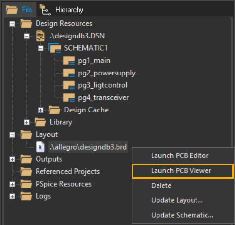
The Allegro Free Physical Viewer opens showing the selected board file.
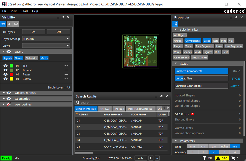
View the next document: 19 - Using Capture with PCB SI
If you have any questions or comments about the OrCAD X platform, click on the link below.
Contact Us