16 - Design Netlisting
Overview
You netlist a design after you place parts, update part references, and check for design rule violations.
You can choose from more than 30 industry-recognized netlist formats. Your choice of netlist format is determined by the application that you intend to use.
The EDIF 2 0 0, VHDL, PSpice and Verilog netlist formats generate true hierarchical netlists. When a design is netlisted with one of these formats, the instance property values on nets and parts are used. All other netlist formats in Capture produce flat netlists, and use occurrence property values.
If you have translated a design with multiple schematic folders, use Annotate (and check for duplicate references) before netlisting.
Note:
- Run Design Rules Check to verify your design before you generate a netlist. This allows for more efficient netlist creation, and you can concentrate on netlist-specific problems if they should occur during the Create Netlist process. Design Rules Check warns you if certain conditions exist in your design. The severity of the specific problem may prevent completion of the design. Other conditions are subject to your judgment, and may be of no consequence. If you are satisfied with the results of design tests such as Design Rules Check, then proceed with the creation of a netlist.
- Design Rules Check uses the decision matrix located in the ERC Matrix tab located in the Design Rules Check dialog box. It also uses a set of pre-determined rules, which are part of the executable code.
- Use Design Rules Check as a guide to verify the integrity of your design. It is only a guide. It is possible to generate a valid netlist even if Design Rules Check reports errors.
- The value, if any, you create for the PCB footprint depends on the particular netlist format you want to produce. Different applications require netlists with different types of PCB footprints. If you do not specify this property, the PCB footprint will be set to the part value.
When you are creating schematic pages, you can assign a variety of aliases to signals that are ultimately connected, but the netlist needs exactly one name for each net.
Net Name Resolution
If Create Netlist encounters multiple names for a single net, higher priority aliases override lower-priority aliases. Priority is determined by the source of the name, ranked as follows:
|
Lowest: |
System-generated names |
|
Highest: |
Named nets |
Any remaining conflicts among netnames are resolved according to the following rules:
- The net name closest to the "root" of the project takes precedence over those further away.
-
If the net is a bus, the net alias assigned to the greatest number of bus members has the highest priority.
Note: To transfer the bus to PCB Editor, ensure that you assign the
BUS_NAMEproperty to the bus or individual members of the bus. - Among net names of equal precedence, priority follows an alphabetical order.
As you can see, a net may change names several times as Create Netlist works. For example, the net may start with an alias of Battery on one page, be renamed ToBattery from an off-page connector, change again to become DC as a port is encountered, and finally change to BatteryBackup when Create Netlist finds a named net closer to the root schematic folder. Once the netlist is created, you can select any piece of the net anywhere in the design and see the net's name as it is recorded in the netlist (BatteryBackup), not as it appears at that particular location.
NETLIST_IGNORE Property
The NETLIST_IGNORE, a reserved property, is attached to component instances. When you set this boolean property to TRUE, the component instance does not appear in the Allegro netlist.
PACK_SHORT Property
Capture includes a PACK_SHORT property that lets you map one logical pin to two or more physical pins. Take the example of an SMA connector. It has one signal pin and 4 shielding pins connected to Ground. The standard Capture symbol has only one visible Ground pin. So what is required is to short all the 4 GND pins in the Allegro netlist with the net that is connected to the visible GND pin.
To do this, you can either add the other three Ground pins as NC or with a different net name depending on whether they have been added as invisible or visible with zero stub length.
Alternatively, you can use the PACK_SHORT property in Capture to hide the PACK_SHORT pins or make them visible with zero length pin stub.
Using this property, multiple groups of pins, each group having two or more pins, can be shorted.
Syntax:PACK_SHORT=(<group1>)(<group2>)[<group3>]
Where: <group> indicates (logicPin1, logicPin2 ... [logicPinN])
Example
Consider the assignment, PACK_SHORT = (A1, B1, Y1) (A2, B2) shorts together. The nets attached to logic pins A1, B1, and Y1 are shorted with each other and the nets attached to pins A2 and B2 are shorted with each other.
The PACK_SHORT property is implemented so you can either hide the pins to be shorted by checking the ignore checkbox in the Package Properties dialog box or you can make them zero length pins and show them as unconnected as illustrated below.
Method 1: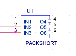
The above part has O4, O5 and O6 added as PACK_SHORT pins (IN1,O4,O5,O6) that will inherit the pin IN1 net set as zero-length but their stub will still be visible. If you instantiate this part and generate an Allegro netlist, IN1, O4, O5 and O6 will inherit the same net.
If IN1 is left unconnected, all PACK_SHORT pins will be marked as NC.
Method 2: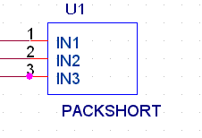
If you have chosen to hide the pins to be shorted by checking the Ignore checkbox in Package properties, and also defined those pins as part of the PACK_SHORT property, the hidden pins will be written to the netlist. Also, its net will be inherited from the master pin that is visible on the symbol instance.
You can also use the PACK_SHORT property in conjunction with the PSpiceOnly property to specify shorting for nets attached to the instance. If a PACK_SHORT device is connected with two different nets across the PACK_SHORT pins, the net connected to the first pin defined in PACK_SHORT property will be written to the netlist.
Create Netlist Dialog Box Tabs
OrCAD X Capture supports a number of netlist format files. You choose a netlist format in the Create Netlist dialog box.
.DLL files, while SDT netlist format files are provided as .EXE files.Creating a Netlist
To create a netlist, do the following:
- In the project manager, select the design file for which you want to create a netlist.
-
Choose the Tools – Create Netlist menu to display the Create Netlist dialog box.
- In the Create Netlist dialog box, select a tab corresponding to the netlist format you want to use.
- In the Netlist File field, enter a name for the output file. If the selected format creates an additional file (such as a map file or pinlist file), enter the filename in the appropriate field.
If necessary, set the Part Value and PCB Footprint combined property strings to reflect the information you want in the netlist. For more information about combined property strings, see Combined property strings.
If necessary, set other format-specific options in the Options group box. - Click OK to create the netlist.
Creating a Flat Netlist
To create a flat netlist, do the following:
- In the project manager, select the design file (
.DSN) to netlist. - From the Tools menu, choose Create Netlist.
- Select the PSpice tab.
- Leave all the check boxes in the Options group blank.
- In the Use Template list box, select the netlisting template(s) to apply.
Check whether you want to place DRC markers for Errors and Warnings. - In the Netlist File field, enter a name for the output file, or click the Browse button to assign a filename.
If required, click the View Output check box to display the netlist after it is generated. - Click OK.
Generating a Layout Editor Netlist
To forward annotate information from Capture to a layout editor, such as PCB Editor or OrCAD X Presto, do the following:
- In the Capture project manager, select the design for which a layout editor netlist is to be created.
- Choose the Tools – Create Netlist menu.
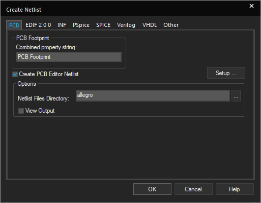
- In the Create Netlist dialog box, select the PCB tab.
- Ensure that the Create PCB Editor Netlist check box is selected.
- Select the Setup button.
- In the Setup dialog box, ensure that the correct configuration file is specified in the Configuration File text box.
By default,<installation_directory>\tools\capture\allegro.cfgfile is used. However, if you want to use a custom configuration file, specify its the path in the text box. - To ignore the electrical constraints during netlisting, select the Ignore Electrical constraints check box.
The following constraints are ignored:
PROPAGATION_DELAYRATSNEST_SCHEDULERELATIVE_PROPAGATION_DELAYDIFFERENTIAL_PAIRNET_SPACING_TYPENET_PHYSICAL_TYPEELECTRICAL_CONSTRAINT_SETRATSNEST_SCHEDULEVOLTAGEMIN_LINE_WIDTHMIN_NECK_WIDTHMATCHED_DELAY
- To suppress the netlisting warnings during the netlisting process, enter the warning (for example
ORCAP-36006) you want to suppress in the Suppress Warnings text box and click Add to add the warning to the list of warnings to be suppressed. - Specify the value of other fields as required and click OK.
- In the Setup dialog box, ensure that the correct configuration file is specified in the Configuration File text box.
- In the Netlist Files Directory text box, enter the folder name where the generated netlist is to be saved.
- Select the View Output check box to open the generated netlist files in Capture GUI.
- Click OK.
The warnings and errors generated during the netlist process are listed in the Session Log window.
An error will be generated during netlisting if a part has an invisible power pin and the device property for the part has Power Pins Visible checked.
Capture netlister generates the following three netlist files compatible with PCB Editor and OrCAD X Presto.
PSTCHIP.DAT: This file contains a description for each different type of part used in the design. The netlister extracts this information from the properties on occurrences.PSTXNET.DAT: This connectivity file, also referred to as the flat list or expanded net list, contains each net, its properties, its attached nodes, and node properties. The list is ordered by physical net name.-
PSTXPRT.DAT: This file, also referred to as the expanded parts list, contains a list of physical parts and lists each reference designator and the sections assigned to it, ordered by the reference designator and the section number
Working with Hierarchical Netlists
Creating a Hierarchical Netlist
To create a hierarchical netlist, do the following:
- In the project manager, select the design file (
.DSN) you want to netlist. - Choose the Tools – Create Netlist menu command.
- Select the PSpice tab.
- In the Options group, click Create Hierarchical Format Netlist.
- Click Settings to customize the format of the hierarchical netlist.
- Click Create Subcircuit Format Netlist to specify how subcircuits will be netlisted.
- In the Use Template list box, select the netlisting template(s) you wish to apply.
- Check whether you want to place DRC markers for Errors and Warnings.
- In the Netlist File text box, type a name for the output file, or click the Browse button to assign a filename.
If required, click the View Output check box to display the netlist after it has been generated. - Click OK.
Customizing a Hierarchical Netlist
You can also customize the format of the subcircuit definition and reference text in the netlist. After these settings are defined, they persist and apply to all subsequent PSpice netlists whether the netlist is invoked from the Tools menu in the project manager or directly from within the schematic editor. You can change the settings in the Settings dialog box.
Two groups of settings are saved: PSpice and Layout versus Schematics (LVS). Having two groups makes it easy to switch between netlisting for PSpice and netlisting for an LVS-compatible format. You can specify which group of settings is active for the netlister by using the Products list box.
To customize the hierarchical netlist, do the following:
- In the PSpice tab of the Create Netlist dialog box, click Create Hierarchical Format Netlist under the Options group box.
- Click Settings, then enable or specify the options, as desired:
- Click OK.
Passing parameters to subcircuits
Hierarchical netlists have the advantage of allowing parameters to be passed from the top-level schematic to any subcircuit schematics. To use this feature, use the SUBPARAM part in the SPECIAL.OLB library.
To learn more about setting up parameterized subcircuits for hierarchical netlists.
During hierarchical netlist creation, a message might display indicating that occurrence properties are being ignored, 'Occurrence-specific properties on <part name>, ignoring.'. No components are ignored in this case.
This message appears only during hierarchical netlist creation. There might be scenarios when the same hierarchical block is instantiated more than once on the schematic. The underlying components inside hierarchical block might have different values or properties (by virtue of occurrences). A hierarchical netlist creates just one subcircuit for both the replicated hierarchical blocks, and call that subcircuit multiple times in netlist based on the number of instances of the block . The underlying component values considered for the netlist are instance values and not occurrence values because only one subcircuit is being created by the netlister.
This message flags for all the components inside the hierarchical block, which has occurrence properties different from instance properties.
Creating Subcircuit Netlists
You can specify how subcircuits in a hierarchical design are processed and defined in the simulation netlist.
You cannot directly simulate a subcircuit netlist; it defines a model that can be called by another circuit being simulated. The models of parts in the PSpice libraries such as op amps and regulators, which have multiple constituent components, are implemented as subcircuits.
A subcircuit implementation may consist of a single schematic, or a hierarchy of schematics.
To create a subcircuit format netlist
- In the project manager, select the design file (.DSN) you want to netlist.
- From the Tools menu, choose Create Netlist to display the Create Netlist dialog box.
- Select the PSpice tab.
- In the Options group, click Create Subcircuit Format Netlist, then click one of the following options, as required:
- Descend: This generates a definition of a hierarchical design that includes the top level circuit as well as its subcircuits. (This option is only available if Create Subcircuit Format Netlist is enabled.) If the Create Hierarchical Format Netlist is not checked, then this option combination is equivalent to creating a flat netlist.
- Do Not Descend: This generates a definition of a hierarchical design that includes only the top level circuit, without any of its subcircuits. (This option is only available if Create Hierarchical Format Netlist and Create Subcircuit Format Netlist are enabled.)
To define a subcircuit
- Place hierarchical ports on the top level of the subcircuit for each node that interfaces to the circuit that will use it. (You should place all such ports on a single page of a multi-page schematic.)
- Add a sequence property to each port, assigning values of 1, 2, and so forth. When you select the Create Subcircuit Netlist Format option on the PSpice tab of the Create Netlist dialog box, it generates a header line of the form:
.SUBCKT LM317 IN ADJ OUT
The example above comes from a schematic with ports named IN, ADJ, and OUT. The three ports were assigned Sequence property values of 1, 2 and 3 respectively.
To use this subcircuit in another schematic
- Place a hierarchical symbol, or draw a hierarchical block.
- Set the Implementation Type to PSpice Model and the Implementation to LM317. The symbol or block must be primitive and have a PSpice Template such as the following:
X^@REFDES %IN %ADJ %OUT @MODEL
The PSpice netlister, under guidance of the PSpiceTemplate, produces a line of the form:
X_U1 INNET ADJNET OUTNET LM317
INNET, ADJNET and OUTNET refer to the IN, ADJ, and OUT ports of the defining circuit. Because the correspondence is by position, the port order in the subcircuit definition must match the net order in the reference. The order in which netnames appear in the reference is controlled by the PSpiceTemplate property. As mentioned above, the Sequence property added to each port determines the order in which port names appear in the subcircuit definition.
For more information on the use of subcircuits, see the section on the .SUBCKT command in the online PSpice Reference Manual.
Using SUBPARAM
You can pass parameters from the top-level schematic to a subcircuit schematic using the SUBPARAM part. This allows you to explicitly define the properties and default values to be used during netlisting and simulation.
Any part in the subcircuit (child) schematic can reference the properties in its PSPICETEMPLATE. The PSpice subcircuit mechanism supports parameterizing:
- constants specified on device statements
- model parameters
- expressions consisting of constants
- parameters
- functions
To set up parameter passing to a subcircuit using SUBPARAM, do the following:
- Make the subcircuit your active schematic page in the Capture schematic page editor.
- From the Place menu, choose the Part command.
- Select the part SUBPARAM from the PSpice library
SPECIAL.OLBand place it on the subcircuit. - With the SUBPARAM part still selected, from the Edit menu, choose Properties.
The property editor appears.
In the spreadsheet, on an instance-by-instance basis, define the names and default values for the properties that can be changed. - To view property names and values at the same time, select a property cell, and click the Display button.
- The Display Properties dialog box displays.
- Check Name and Value format for Display Format, then click OK.
In the top-level schematic, use the property editor to edit the properties of the hierarchical part or block that references the subcircuit (child) schematic so they match the properties you defined in Step 5.
Example
This fourth-order Chebyshev filter schematic illustrates how the SUPARAM part may be used to pass design parameters from a top-level (parent) schematic to a subcircuit (child) schematic in a hierarchical design.
In the top-level schematic, you explicitly define the parameter values you want to pass to a subcircuit. In this case, the parameters and their corresponding values for the U2 subcircuit are Rin = 110 and Rfeedback = 22.1k.
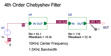
Descending into the hierarchy of the U2 subcircuit, you see the Rin and Rfeedback parameters listed with their corresponding default values of 100 and 20k, respectively, in the SUBPARAM part (under SUBPARAMETERS).
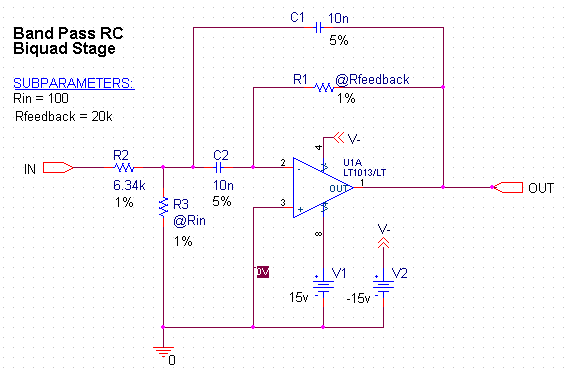
Notice the Rin and Rfeedback values are preceded with @ symbols, indicating that these parameters are substituted with values passed down from the top-level schematic.
Here is the hierarchical netlist generated in Capture for this design:
* source HISTO
V_V1 N00023 0 AC 1v
X_U1 N00023 N00030 OneStage PARAMS: RIN=93.1 RFEEDBACK=18.2k
X_U2 N00030 OUT OneStage PARAMS: RIN=110 RFEEDBACK=22.1k
.SUBCKT OneStage IN OUT PARAMS: RIN=100 RFEEDBACK=20k
V_V2 V- 0 -15v
R_R2 IN N00024 R_R2 6.34k
.model R_R2 RES R=1 DEV=1%
R_R1 N00034 OUT R_R1 {Rfeedback}
.model R_R1 RES R=1 DEV=1%
R_R3 0 N00024 R_R3 {Rin}
.model R_R3 RES R=1 DEV=1%
C_C1 N00024 OUT C_C1 10n
.model C_C1 CAP C=1 DEV=5%
C_C2 N00024 N00034 C_C2 10n
.model C_C2 CAP C=1 DEV=5%
X_U1A 0 N00034 N00594 V- OUT LT1013/LT
V_V1 N00594 0 15v
.ENDS
Here, the U2 and U1 subcircuits are referenced in the source (top-level) circuit as X_U1 and X_U2 with the explicit values defined for the parameters that are passed to from the top-level. A .SUBCKT models both the U1 and U2 subcircuits and the default parameters are listed as placeholders. When PSpice simulates the design, the parameters passed from the top-level circuit are the ones used in the subcircuits.
Specifying an Alternate Netlist Template
To specify an alternate netlist template
- In the Capture project manager, select the design file (.DSN) you want to netlist.
- From the Tools menu, choose Create Netlist.
- Select the PSpice tab.
- In the Use Template list box, add the name of the template to use.
View the next document: 17 - Simulating Capture Designs Using PSpice
If you have any questions or comments about the OrCAD X platform, click on the link below.
Contact Us