13 - Design Annotation
Overview
Annotating a design involves assigning reference designators and net names to unnamed parts and electrical connections in your design. By annotating your design, you provide the means by which to pass it downstream to other layout design tools, such as OrCAD X PCB Expert (classic PCB editor) and OrCAD X PCB Layout (new interface), that take it beyond the schematic creation phase of the design. Some of the downstream applications include PCB layout tools, simulators, and logic optimizers.
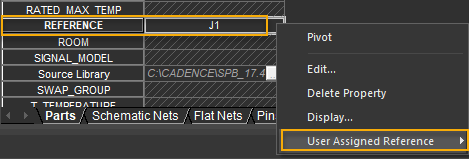
If the instance and occurrence values are the same in a hierarchical design, this command cannot set the flag for an occurrence value. If you want to set the User Assigned Flag for the occurrence value, edit the Reference value and then set the flag.
U1A, U1B, U1C in a design, and run annotation with Reset part references to ? option selected and Preserve designator option unselected, the designator information is lost in the design. To preserve designator information of a design, select Preserve Designator option in the Annotate dialog box before running annotation.Customizing Part References in a Design
You can customize the way Capture assigns part references in your design. You can specify a range of part reference values that Capture uses to annotate a schematic page or a hierarchical block in your design. Use the Annotate dialog box to complete this task.
To customize part references in a design using either schematic page-wise or hierarchical block-wise annotation, do the following:
-
In the project manager, select the design file, schematic folder, or a schematic page.
Capture currently does not support the specifying of part reference range for a portion of the design, for example, a specific schematic page or a schematic folder. You need to specify a part reference range for all the schematic pages or hierarchical blocks in your design. - Choose the Tools – Annotate menu command.
The Annotate dialog box appears.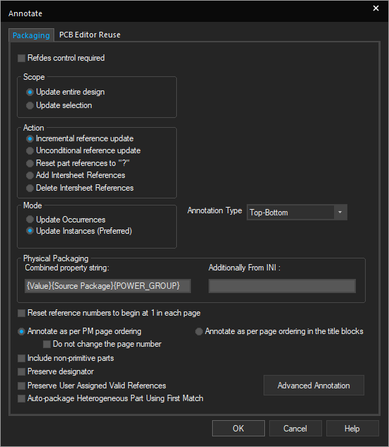
- Select the Refdes control required check box to specify a part reference range for each schematic page or a hierarchical block in your design.
The Scope options in the dialog box change to Schematic Pages and Hierarchical Blocks. Also, a grid appears on the right-hand side of the dialog box displaying all the schematic pages or hierarchical blocks in the root schematic folder of your design depending on whether your design is a flat design or a hierarchical design.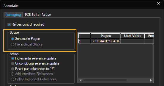 Schematic Page-Wise Annotation
In schematic page-wise annotation (recommended for flat design), you can set a part reference range for each schematic page that exists in the root schematic folder of your design. All the schematic pages in the root schematic folder are displayed in a grid in the Annotate dialog box in the following format:
Schematic_Folder_Name:Schematic_Page_Name.Hierarchical Block-Wise Annotation
In hierarchical block-wise annotation (recommended for hierarchical design), you can set a part reference range for each hierarchical block that exists in root schematic folder of your design. All hierarchical blocks in the root schematic folder are displayed in a grid in the Annotate dialog box in the following format: Schematic_Folder_Name:Hierarchical_Block_Name.
The grid is divided into rows and columns. Each row has a number, a schematic page name or a hierarchical block name, and cells to specify the Start and End values for the part reference range.
For example, the Tutorial.dsn sample design, which is a flat design, contains a schematic page defined at the root level of the design, SCHEMATIC1. When you select the Refdes control required check box, the grid displays the following entry in the Pages column: SCHEMATIC1:PAGE1, where SCHEMATIC1 is the root schematic folder name and PAGE1 is the schematic page name.
Consider the example of a hierarchical design, FULLADD.DSN, which contains two hierarchical blocks defined at the root level of the design. When you select the Refdes control required check box, the grid displays the following two entries in the H-Blocks column: FULLADD:FULLADD:halfadd_A and FULLADD:FULLADD:halfadd_B, where FULLADD is the root schematic folder name and FULLADD:halfadd_A and FULLADD:halfadd_B are the reference to the root-level hierarchical blocks in the design. The grid displays only the schematic pages or hierarchical blocks on the root schematic of the design.
 - Enter a numeric value greater than 0 in the Start Value and End Value columns corresponding to each schematic page name or the hierarchical block name.
– Use the
Tabkey to move from the Start Value column to the End Value column.– You can also use the Arrow keys to move around in the grid.
– You can use the column handle (
 ) to resize the rows and columns in the grid.
– A valid range must have both the Start and End Values, and End Value must be greater than the Start Value.
- Specify all the other desired settings in the Annotation dialog box.
If you set the design for schematic page-wise or hierarchical block-wise annotation and also use the:- Incremental reference update option, all the part references in your design are updated incrementally within the specified part reference range. However, this does not affect the existing annotated parts in your design.
- Unconditional reference update option, all the part references in your design are updated unconditionally from the start value specified in the part reference range.
 Additionally, Capture flashes error and warning messages if it encounters any invalid operation while using this functionality. For example, the same part reference range for more than one schematic page or hierarchical blocks in your design or parts in your design that are outside the specified part reference range.
 - Click OK.
Part references in each schematic page or hierarchical block are updated according to the range specified for them in the Annotate dialog box.
- Capture saves the annotation preferences for the project when you click OK. These settings are used whenever the project is opened next.
- If you are using the Refdes control required option for a project, the Auto reference placed part option in the Miscellaneous tab of the Preferences dialog box does not honor the range specified in the grid.
- If any changes are made to the root schematic of a design, all the part reference range values specified in the grid for the design are lost. However, this does not affect the existing annotated parts in the design.
Backannotating
You use backannotation to transfer packaging information to your schematic folder from other EDA tools. Using the Tools – Back Annotate command, you can import changes created by external tools, such as PCB layout editors. To backannotate properties, you use the Update Properties tool. Capture uses a simple file format to provide support for gate swapping, for pin swapping, and for changing or adding properties on parts, pins, or nets. If the external tool creates a backannotation file, edit the file to match the format described inDesignating pins, gates, or packages for swapping.
Example
You might backannotate a design. After you complete your schematic design and while you are routing a printed circuit board, you realize that you can greatly reduce the via count, track length, or routing complexity by exchanging two of the gates or pins on a part. You use your board layout application to rewire the board, exchanging the connections of U1A and U1B. To ensure that your schematic design reflects the changes, you use a text editor to create a swap file, then run the Back Annotate command. The next time you look at the design, you see that U1A and U1B have swapped places.
Backannotating board file information to your schematic design involves creating a report file and reading it back into Capture
To backannotate schematic information, do the following:
- After making changes to the design in the layout tool, choose the File – Reports menu command.
The Generate Reports dialog box appears. - If you re-annotated the names of parts, or altered parts or nets, choose OrCAD backannotation file (
.SWP) to create a combined swap and update file. - Click OK to create the report.
- In Capture, from the project manager, choose Tools – Back Annotate.
The Backannotate dialog box appears. - Use the Browse button to find the file (
.SWP) you created in step 2, and click OK.
Capture updates the schematic design.
To backannotate part packaging information, do the following:
- Using a text editor, create a swap file.
See Designating pins, gates, or packages for swapping for details. - In the project manager, select schematic folders or schematic pages to process only a portion of the design. To process the entire design, leave the schematic folders or schematic pages unselected.
- Choose Tools – Back Annotate.
The Back Annotate dialog box displays. - In the PCB Editor tab, verify that the required options are set.
For example, check the name and location of the netlist directory and the swap file. - Click OK.
Shortcut
Toolbar: 
Selecting Annotation Sequence
You can select the sequence in which the components of your design are annotated.
To select the annotation sequence, do the following:
- Choose Tools – Annotate from the main menu.
- In the Annotate dialog box, select the Annotation Type drop-down button.
The Annotation Type list contains three options that you can use to decide the sequence in which the objects on your design are annotated: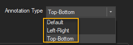
- Select the desired option from the list.
Example
To differentiate between the way these sequences work on a design, see the following example of a dense design that contains a number of large components clustered together. Notice the sequence of annotation of the components on the design in each case.

- Annotating the design with the Default Annotation Type option selected leads to the following results:
- Annotating the design with the Left-Right Annotation Type option selected leads to the following results:

The annotation procedure using this option scans the page grid from left to right one grid line at a time, and then moves downwards to the next grid line. In effect, the sequence is left to right and top to bottom.
- Annotating the design with the Top-Bottom Annotation Type option selected leads to the following results:
 In this case, the procedure scans the pages from top to bottom one grid line at a time, and then moves towards the left of the screen.
Swap File
For PCB designs, a swap file (.SWP) is a text file containing old and new part references for use with the Back Annotate command. Swap files are typically created by another application, such as PCB Editor.
SWP extension.Contents of a Swap File
A swap file contains the following elements:
- The file can include comments. During backannotation, any text to the right of a semicolon is ignored.
Example:CHANGEREF U1 U2 ;Change part reference U1 to U2 - In a swap file, each line (unless preceded by a semicolon) causes one action.
Example:GATESWAP U1 U2 ;Change part U1 to U2 and ; part U2 to U1CHANGEREF U1A U1B ;Change part reference U1A to U1B - The elements of each line may be separated with any number of space or tab characters.
Example:PINSWAP U3 5 6 ;Swap pins 5 and 6 on U3 - In general, the first element of the line specifies the type of swap. If no swap type is specified, the default type CHANGEREF is assumed. The other swap types are GATESWAP, PINSWAP, and CHANGEPIN.
Example:CHANGEREF U1A U1B ;Change part reference U1A to U1BGATESWAP U1A U1B ;Swap gates A and B on U1PINSWAP U5B "D0" "D1" ;Swap the pins named D0 and D1 on U5BCHANGEPIN U5B "D0" "D1" ;Changes pin D0 to D1 on U5B
Considerations when Creating a Swap File
Include only the changes from the current state of the design to the desired state. For example, you might place a part as U1 in the design, and change it in a PCB layout package first to U2, then to U3. The swap file should reflect the change from U1 to U3; do not include the intermediate step involving U2.
- For gate swaps, ensure that the gates being swapped are of the same type. Unmatched gate types might lead to incorrect results.
- For pin swaps, an additional element — the part reference — must be specified before the old and new values. A pin swap is limited to the pins of the same type and shape on the same part. For example, you can swap data pins on
U5B, but you cannot swap a pin onU5Bwith a pin onU5C.
CHANGEREF
Changes the reference of the specified part.
Examples
CHANGEREF U1 U2 ; Change part reference U1 to U2
CHANGEREF U1A U1B ; Change part reference U1A to U1B
U1C U2B ; Change part reference U1C to U2B
GATESWAP
Swaps the specified parts or packages. If U1 and U2 are multiple-part packages, all the devices in U1 will change to U2, and conversely— U1A, U1B, and U1C change to U2A, U2B, and U2C, respectively. Similarly, U2A, U2B, and U2C change to U1A, U1B, and U1C, respectively.
Examples
GATESWAP U1 U2 ; Change part U1 to U2 and
 ; part U2 to U1
GATESWAP U1A U1B ; Swap gates A and B on U1
GATESWAP U1C U2B ; Swap gates U1C and U2B
GATESWAP U1C U2B ; Swap gates U1C and U2B
PINSWAP
Swaps two pins on the specified part. Only pins of the same type and shape on the same part can be swapped. A pin is identified by a name or a number. A pin name must be enclosed in double quotation marks. PINSWAP can be used multiple times on the same pins in a swap file.
Examples
PINSWAP U5B "D0" "D1" ; Swap the pins named D0 and D1 on U5B
PINSWAP U3 5 6 ; Swap pins 5 and 6 on U3
CHANGEPIN
Changes the first pin with the second pin. Only pins of the same type and shape on the same part can be swapped. A pin is identified by a name or a number. A pin name must be enclosed in double quotation marks. CHANGEPIN can only be used once on each pin in a swap file.
Examples
CHANGEPIN U5B "D0" "D1" ; Changes pin D0 to D1 on U5B
CHANGEPIN U3 5 6 ; Changes pin 5 to pin 6 on U3
Designating Pins, Gates, or Packages for Swapping
To improve board routing, you can designate pins, gates, or packages for swapping.
To specify that pins, gates, or packages in your PCB design are eligible for swapping, do the following:
- Using a text editor, create a swap file. See Creating a swap file (.SWP) for instructions.
- In the project manager, select schematic folders or schematic pages to process only a portion of the design. To process the entire design, leave the schematic folders or schematic pages unselected.
- Choose Tools – Back Annotate.
The Back Annotate dialog box displays. - Verify that the dialog box options are set as required. For example, you specify whether you want to process the entire design or only the selected schematic folders or schematic pages, and the name and location of the swap file.
- Click OK.
Shortcut
Toolbar: 
Example
CHANGEREF U1 U2 ; Change part reference U1 to U2
CHANGEREF U1A U1B ; Change part reference U1A to U1B
 U1C U2B ; Change part reference U1C to U2B
GATESWAP U1 U2 ; Change part U1 to U2 and part U2 to U1
GATESWAP U1A U1B ; Swap gates U1A and U1B
PINSWAP U7 1 2 ; Swap pins 1 and 2 on U7
PINSWAP U5B "D0" "D1" ; Swap the pins named D0 and D1 on U5B
PINSWAP U3 5 6 ; Swap pins 5 and 6 on U3
Update File
The update file is used by the Update Properties functionality to determine the objects to change, the impacted properties of the objects, and the values the properties receive on update.
You create an update (.UPD) file using any text editor that saves files in ASCII format.
Contents of Update File
The update file contains the following elements:
- Header line – The first line of the update file is a header line. It starts with a combined property string that identifies which properties to compare. In the following example, only the
Net Nameproperty is compared. The other strings on the first line specify which properties to update when a match is found. - Comments – Any comment including any text to the right of a semicolon is ignored by the Update Properties tool.
- Strings – All strings in the update file except for comments are enclosed in quotation marks and cannot exceed
124characters. You can use spaces and tab characters to format the update file in rows and columns. - The rest of the file contains lines for each match string to be compared and the values to be recorded in the updated properties.
Example
"{Net Name}" "Track Width" "Net Spacing" "Routing Priority""VCC" "0.04" "0.035" "3" ; Any text to the right
"CLK" "0.01" "0.025" "1" ; of a semicolon is
"CLR" "0.01" "0.025" "3" ; ignored by the
"RESET" "0.01" "0.025" "3" ; Update Properties
"GND" "0.04" "0.035" "2" ; tool.
The combined property string is {Net Name}. For every object whose Net Name property value matches one of the strings in the first column, the following properties are updated with the corresponding values:
Track WidthNet SpacingRouting Priority
For instance, each object for which the Net Name property is set to VCC is updated as follows:
Track Widthproperty is set to0.04Net Spacingproperty is set to0.035Routing Priorityproperty is set to3
Combined property strings
With many of the tools in Capture, such as Create Netlist and Annotate, you use combined property strings to convey information to the tool or to limit the tool's action. A combined property string consists of one or more property names, enclosed in braces, and can also contain literal text. Capture combines the values of the named properties with any literal text to create a string. An example is:
{Value}{Reference}where "Value" and "Reference" are property names. Using this combined property string and a part with a part value of 74LS32 and a part reference of U?A, Capture creates the string:
74LS32U?A
You can include spaces and other characters in the combined property string, as in this example:
Part: {Value} ({Reference})Using this combined property string and the same part, Capture creates the string:
Part: 74LS32 (U?A)
Different tools use combined property strings in different ways. For example, Annotate uses one to compare parts—if one part's combined property string matches another part's combined property string, it packages the parts together.
- Bill of Materials and other commands on the Tools menu that generate an output file based on a combined property string may produce errors if you include extra curly braces.
- You can include tabs in combined property strings, so that the output file can be manipulated in a spreadsheet or database application. Tabs also help format report files, such as those created by the Bill of Materials command. Wherever you want to have a tab in the output file, insert the characters \t (a backslash and a lowercase "t") in the combined property string.
- Do not use {GROUP} as a property name in combined property strings. This may cause problems while annotating your design for a PCB Editor tool, like Allegro PCB Editor. The GROUP property is used in PCB Editor for a specific purpose.
- Except for the header line, update files for Capture have the same format as the update files used by Update Field Contents in SDT. Once you add the appropriate header line, you can use an SDT update file without modification to change individual property values using Update Properties. You can also build on an SDT update file for a more elaborate property update, because Capture can update multiple properties in a single pass.
Creating a Combined Swap and Update File
You can create a file that combines the swap file and update file information. Run Back Annotate to use a combined swap and update file. Swap and update files need to have the same .SWP file extension as normal swap files.
A swap and update file is divided into sections. Each section uses the following general form:
.label utility-name utility-parameters
section-information
.End
where:
label
Specifies the name of a section. A label can be any string combination of letters and numbers, but must always start with a dot (.).
utility-name
Specifies the utility Capture uses for the section.
| Section | Definition |
|---|---|
| Flags | Marks the view of the design, and the design name and path. |
| GateAndPinSwap | A section using this utility behaves the same as a Back Annotate file. |
| UpdateProperties | A section using this utility behaves the same as an Update Properties file. |
utility-parameters
Specifies the parameters of the utility for the section. All utility parameters only apply to the UpdateProperties utility.
| Parameter | Defintion |
|---|---|
| Parts | Specifies that only parts are updated. If both Parts and Nets are specified as parameters, Nets overrides Parts. |
| Nets | Specifies that only nets are updated. If both Parts and Nets are specified as parameters, Nets overrides Parts. |
| OnlyStuffEmpties | Specifies that only empty properties are updated. If a property already contains a value, then it is not modified. If this parameter is not specified, UpdateProperties unconditionally updates all properties. |
| UppercaseCombined | Specifies that a case insensitive match is to be attempted when comparing the match string with the combined property string. |
| UppercaseStuffString | Specifies that the update string will be changed to upper case before updating the property, but after string matching. |
section-information
Specifies the actions the utility performs for the section. If the utility is GateAndPinSwap, these lines use the normal Gate and Pin Swap file format. If the utility is UpdateProperties, these lines use the normal Update Properties file format. If the utility is Flags, the section contains the following lines:
View = design-view
DesignName = path
where design-view is either Logical or Physical, and path specifies the design file name and path. In Capture Release 9 and later, the Logical design-view corresponds to instances, and Physical corresponds to occurrences.
Example
.Label1 Flags
 View = Physical
 DesignName = C:\ORCADWIN\CAPTURE\DESIGN\FULLADD.DSN
End
.Label2 GateAndPinSwap
 GateSwap R1 R2
 PinSwap R3 "1" "2"
 ChangeRef R4 R10
End
.Label3 UpdateProperties Parts
 "{Part Reference}" "Notes"
 "R10" "This used to be R4"
 "R3" "Notice pins 1 and 2 are swapped"
 "R1" "This used to be R2"
 "R2" "This used to be R1"
End
.Label4 UpdateProperties Nets
 "{Net Name}" "Trace Width"
 "VCC_WAVE" "0.040"
 "GND Power" "0.040"
End
Advanced Annotation
The Advanced Annotation feature provides you the capability to do multi-level annotation and property-block based annotation on a Capture Design. The multi-level annotation can be done either on a full design or selectively done on one or more schematic folders or schematic pages.
In this section, following topics are covered:
- Reference Range Assignment
- Selective Annotation
- Property Block based Annotation
Reference Range Assignment
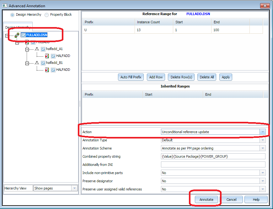
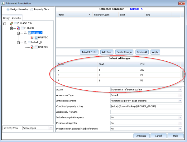
You can assign reference range in the Advanced Annotation dialog box for a complete design, an individual hierarchy block, an individual page in a hierarchy, or a property block.
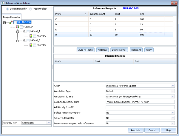
For example, to annotate a complete design. Select the FULLADD.DSN check box in the design hierarchy tab. Once the FULLADD.DSN check box is selected, all the lower-level blocks are automatically selected.
Selective Annotation
If you want to add reference range to a lower block or a child block, the inherited ranges can be seen in the Advanced Annotation dialog box as shown in the following screenshot.
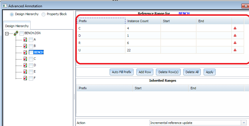
The Auto Fill Prefix button provides you an option to auto-scan the number of prefixes found in a design. Once you click the button, the prefixes' count is automatically filled-up in the Instance Count column of the Reference Range table.
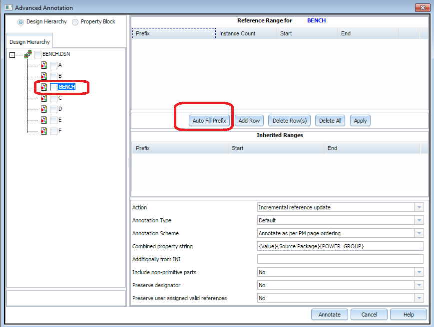
Based on the instance count of each prefix, you can define the reference range.
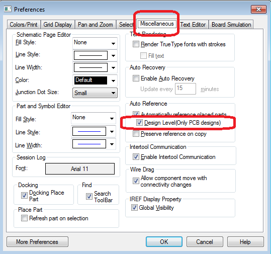
To do auto-referencing during placement of an assigned referenced part or parts, enable Design Level Auto Referencing from Options – Preferences – Miscellaneous Tab.
Property Block Based Annotation
To do Property Block Annotation, you need to select Property Block radio button in the Advanced Annotation dialog box.
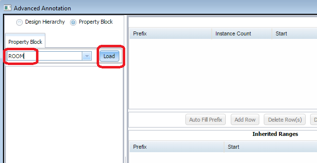
Specify the ROOM property and click the Load button.
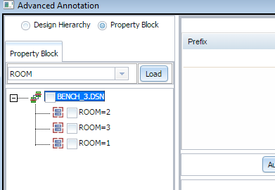
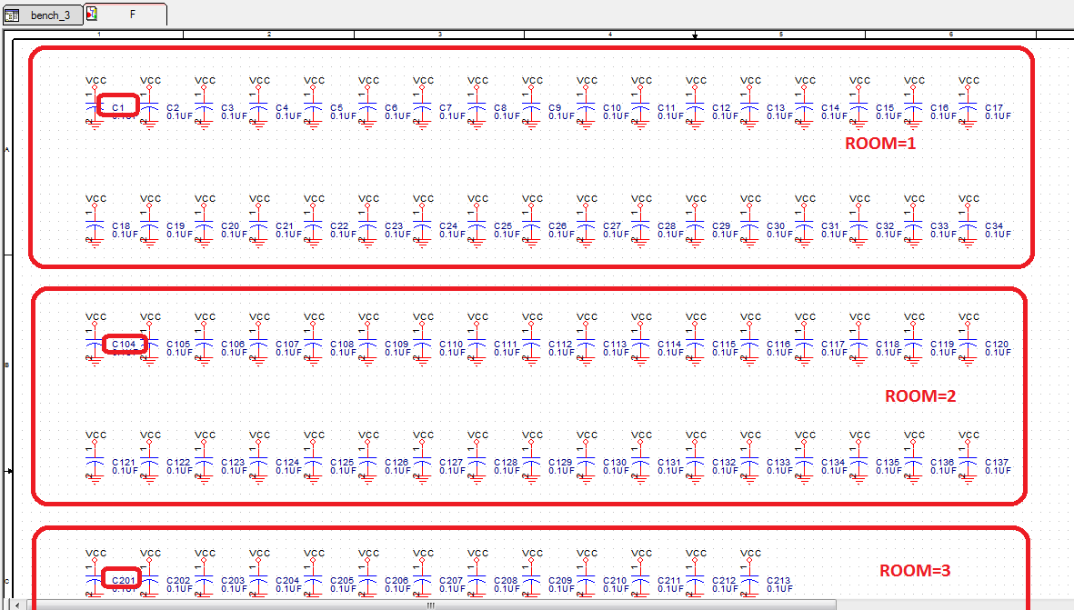
Select each of the property and assign reference range 1 to 100 to the ROOM1 property, 101 to 200 to the ROOM2 property, and 201 to 300 to the ROOM3 property. After annotation is performed, the reference assignment is done according to the property block reference assignment.
View the next document: 14 - Generating Reports
If you have any questions or comments about the OrCAD X platform, click on the link below.
Contact Us