04 - Phases in the Design Flow
Overview
A typical PCB design flow involves the following phases:
- Design Exploration: SigXplorer and Topology Explorer (Not covered in this document)
- Design Capture: OrCAD X Capture, Allegro Design Entry HDL, Allegro System Architect, and Allegro X System Capture
- Floorplanning: Allegro PCB SI
- Implementation: PCB Editor, APD, SiP
Each phase in the design flow requires different tools. Constraint Manager provides a common environment for managing constraints across all tools in the design flow.
Not all phases in the design flow are mandatory. For example, a new design may be a derivative of a prior design. In this case, the exploration and floorplanning phases may not be needed.
Constraint information in the board and in the schematic databases are synchronized using the Design Synchronization tool-set. With Design Sync, you can specify if all the constraints are to be synchronized or only those that have changed.
Contents:
Design Exploration Phase (with SigXplorer)
In the exploration phase, you focus on the exploration before the board is placed and routed. Board cross-section and material type are usually not known, although you can make assumptions from the earlier designs. A netlist is not available in this phase of the design flow.
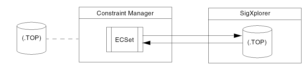
Use SigXplorer to perform simulations based on the ECSets characteristics, such as pins, scheduling, and models. A unique topology template can be saved for each point explored in the solution space. The end result of the exploration phase is to create a library of Electrical CSets (.top files on disk) which can be imported back into Constraint Manager where they can be swapped with other Electrical CSets, or where individual constraints can be moved between Electrical CSets.
In the design exploration phase, constraints can be validated in SigXplorer and saved as topology templates, or they can be defined in Constraint Manager. The primary difference is presentation: SigXplorer is form-based; Constraint Manager is worksheet-based. It is more convenient to use Constraint Manager for viewing and manipulating multiple constraint definitions.
Note that only the Electrical Constraint Set folder is shown in Constraint Manager’s worksheet selector when accessed from SigXplorer. Due to the absence of a board database, and a netlist, Constraint Manager does not show the Nets folder. Similarly, Physical, Spacing, and Same Net Spacing worksheets do not appear.
Also, without a database with which to save constraint data, you must save the constraints to a topology template (.top) to preserve your work, before you exit SigXplorer or Constraint Manager.
This file represents the SigXplorer database. You can later import this information as an ECSet in Constraint Manager.
You also use SigXplorer in the Constraint Manager flow to define custom measurements and custom stimulus.
In SigXplorer, you simulate and analyze the topology. The following can be captured in a topology template:
|
|
|
|
|
Design Exploration Phase - Pin Scheduling
In Constraint Manager, you can select one of the following pre-defined pin scheduling topologies:
- minimum spanning tree
- star
- daisy chain
- source load daisy chain
- far-end cluster
You select these from the Wiring worksheet of the Routing workbook. If you want to define your own pin schedules, you must manually wire the connections in SigXplorer and then export this information back to Constraint Manager (choose File - Update Constraint Manager).
Design Capture Phase - Front to Back Constraint Flow
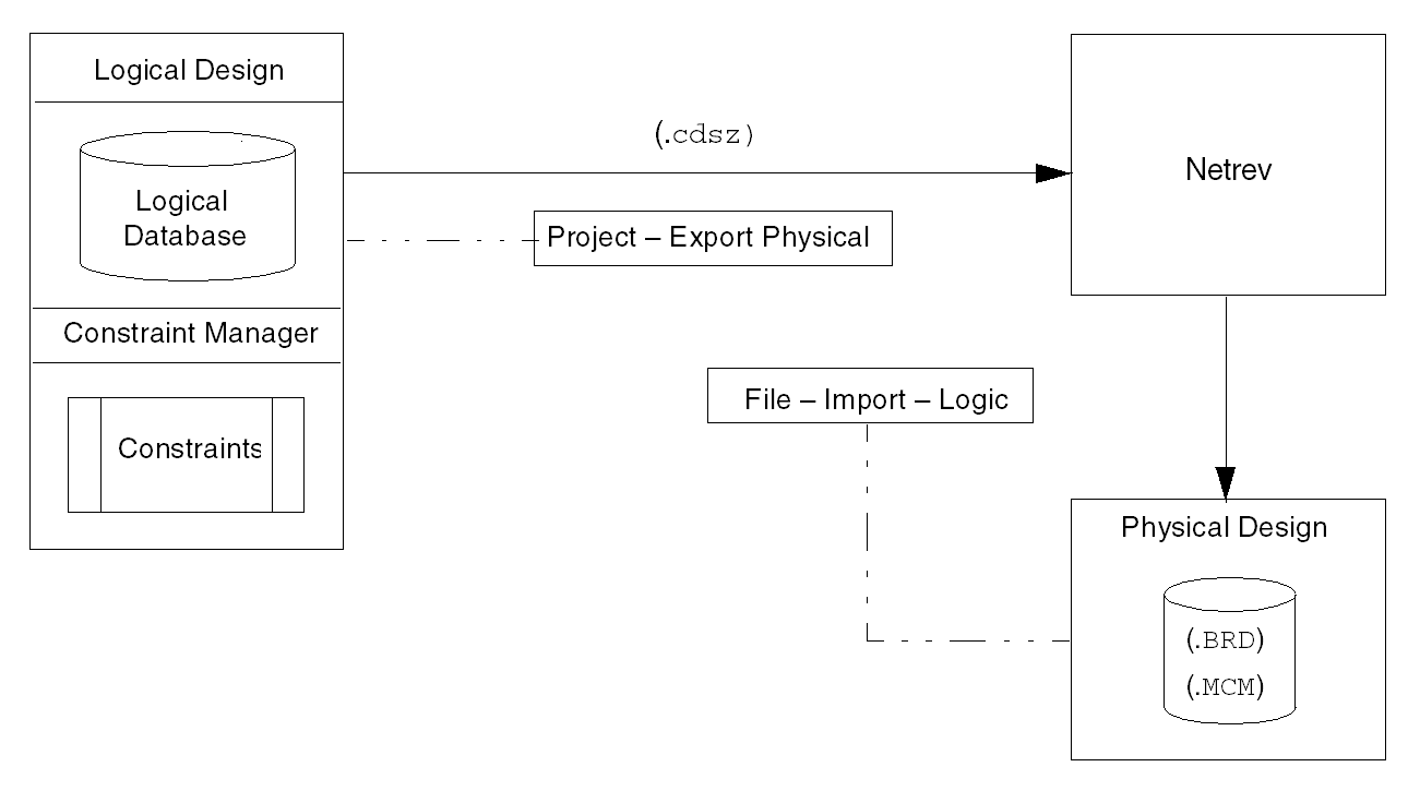
To create a physical layout for the design, the design data and constraint information is exported from the schematic editor to the physical database of PCB Editor. For example, in System Capture design data is exported using File - Export - Export to Layout.
Export Physical extracts five package files -- which communicate logic, part, pin, reference designator, and constraint information -- and writes to the (.cdsz) file. This file is then used by Netrev for back-end processing.
The design capture tools pass electrical, physical, and spacing constraint modifications (and net classes) to the physical design tools for layers that exist in the physical database, or a new, empty physical database seeded from the information passed from a design capture database.
In the front-to-back flow, Design Editor generates the composite file, pstdedb.cdsz, which contains the following package files:
| This file . . . | Contains . . . |
|
|
Physical information for each type of symbol read from the Device files are the third party equivalent of this file. |
|
|
A netlist that uses keywords (net_name, node_name) to specify the reference designators and pin numbers associated with each net. Constraints added to nets using Constraint Manager are written to the pstcmdb.dat file. |
|
|
Contains each physical package or part in the logic design along with its reference designator and device type. For packages or parts composed of multiple logic gates, the file identifies the gate placed in a specific section of the package or part. Also contains attributes of parts and functions, and pin attributes specifically used for packaging. All the other pin attributes (constraints) are written to the |
|
|
Contains constraint and property information for the design. |
Design Capture Phase - Back to Front Constraint Flow
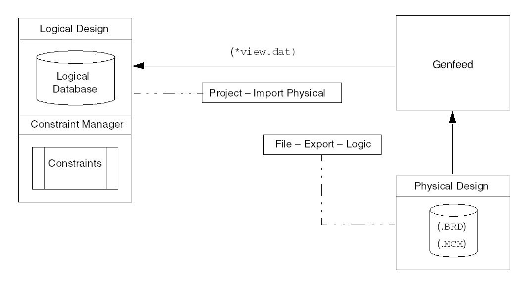
Import Physical is a prescribed set of processes that reconciles design data and constraints between physical and logical databases.
The physical tools pass constraints to the logical database. Physical and Spacing constraints, objects, and layers also make the transition to reconcile both the databases.
Import Physical calls the Genfeed tool to extract six view files -- which communicate component, part, function, pin, and constraint information and passes this file for front-end processing.
| This file . . . | Contains . . . |
|
|
Component information and properties, as defined in the physical tools. |
|
|
Function information and properties, as defined in the physical tools. |
|
|
Connectivity information, as defined in the physical tools. |
|
|
Pin information and package-related properties, as defined in the physical tools. |
Design Floorplanning and Implementation Phases
In the floorplanning and implementation phases, you focus on placement, routing, and manufacturing output. This section focuses on using Constraint Manager with back-end tools.
Constraint Manager is used along with the physical editor to manage constraints. Constraint creation or modifications in Constraint Manager is automatically synchronized with the board (.brd) database.
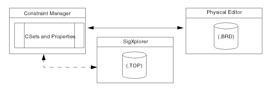
You can also use SigXplorer to perform simulations based upon the ECSet characteristics (pins, scheduling, models) of the net-related objects in the design.
- Launch Constraint Manager from the physical editor (choose Setup - Constraints - Constraint Manager).
- Launch SigXplorer from Constraint Manager by selecting a net-related object (or an Electrical CSet) and choosing Tools - SigXplorer. You can also right-click and choose SigXplorer.
In the floorplanning and implementation phases, you use Constraint Manager to:
- Import reusable topology templates from SigXplorer. These map to Electrical CSets in Constraint Manager.
- Consolidate individual nets and Xnets into more easily-managed units, such as buses and match groups.
- Define bus, differential pair, net, Xnet, or pin pair constraints.
- Define differential pairs.
- Define net-related constraint overrides, as required.
- Create CSets based on net-related objects, such as buses, differential pairs, nets, and Xnets.
- Explore net topologies and schedule pins.
- Audit CSets to resolve inconsistencies.
- Validate the design through design rule checks and analysis.
- Communicate layout changes to design capture tools.
- Open a partitioned design. Sections of the design that are partitioned are not editable, and open in Constraint Manager in read-only mode as indicated by cross-hatch shaded cells. You can analyze a partitioned design in Constraint Manager, but you cannot import constraints.
Using SigXplorer in the Design Capture, Floorplanning and Implementation Phases
Constraint Manager, when launched from a logical editor, does not support topology exploration with SigXplorer and database synchronization.
Unlike in the exploration phase, where there is no board or netlist available, SigXplorer employs a different use model in the floorplanning and implementation phases.
Use SigXplorer to extract a net (or a net-related object, such as a bus, differential pair, or match group) for topology exploration and constraint modification. The extraction can be routed (a trace in the PCB) or unrouted (a ratsnest). Used in this way, SigXplorer is aware of the electrical and physical characteristics of the net.
You also use SigXplorer in the Constraint Manager flow to define custom measurements and custom stimulus.
- SigXplorer extracts all the electrical constraint and topology information from the selected object.
-
If the Use Include Routed Interconnect check box is selected (choose Tools - Options in Constraint Manager), interconnect details (clines and vias) are also included.
You cannot update Constraint Manager with a topology that contains traces or vias. You must condition the topology for Constraint Manager by choosing Edit - Transform - for Constraint Manager in SigXplorer.
- If the Schedule Based on Routed Interconnect check box is selected (Tools - Options in Constraint Manager), the extraction derives connections from the user-defined net schedule (or from the default net schedule if none is specified). SigXplorer derives propagation delay and impedance from traces. Any unrouted segment derives its impedance and propagation velocity from the default settings.
- If the Selected object is a Bus or Differential Pair, the template will include information from the first Xnet or Net.
-
- Display the appropriate ratsnest based on the selected topology schedule:
- for pre-defined scheduling, the value of the RATSNEST_SCHEDULE property is used.
- for user-defined scheduling, the value of the TEMPLATE property is used.
View the next document: 05 - Constraint Analysis
If you have any questions or comments about the OrCAD X platform, click on the link below.
Contact Us