High-Speed Signal Analysis: Design Tips
Key Takeaways
-
Effective high-speed signal analysis ensures impedance matching, minimizing overshoot, undershoot, and signal reflections.
-
Properly manage transmission lines using series termination resistors and impedance matching networks.
-
Leverage powerful OrCAD X tools for real-time signal analysis, impedance control, and advanced routing.
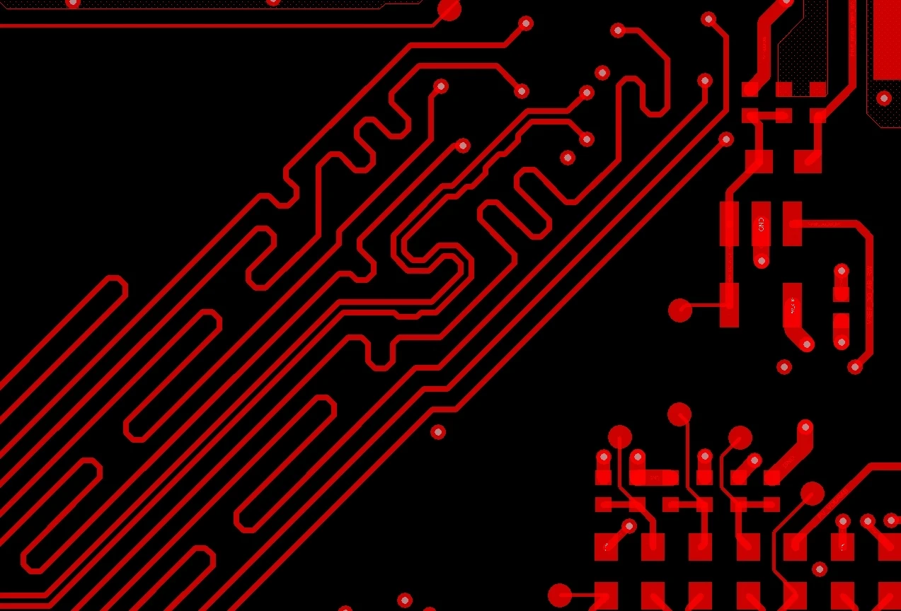
Length matching for high speed design
High-speed PCB design is becoming increasingly more prevalent. With the rise of fast logic families like TTL, simple PCB layouts no longer suffice for maintaining signal integrity. As devices now operate at nanosecond speeds or faster, designers must adopt high-speed techniques to avoid signal artifacts, keep data synchronized, and manage transmission line effects through high-speed signal analysis. Proper grounding and layer stack design are also essential, especially for devices with wireless capabilities or external analog interfaces. Read on as we discuss these aspects of high-speed PCB design, high speed signal analysis, and more, to ensure reliable performance.
High-Speed Signal Analysis Design Considerations
|
Design Aspect |
Tips |
|
Interconnect Design |
Design interconnects with impedance-controlled routing, proper stackup, length matching, and termination networks to prevent signal integrity issues like overshoot and undershoot. |
|
PCB Stackup |
Route signal traces directly over a ground plane, and place inner signal layers between solid copper planes for EMI shielding and crosstalk prevention. Segregate analog and digital sections carefully. |
|
Transmission Line Effects |
Treat traces as transmission lines when their length exceeds one-quarter of the signal rise time. Use series termination resistors at the load to suppress ringing and ensure proper impedance matching. |
|
Clock and Signal Skew |
Precisely match trace lengths in parallel data signals and with clocks to prevent timing skew and bit errors. |
|
Parasitic Capacitance and Inductance |
Minimize parasitic effects by routing traces close to reference planes or as differential pairs. Maintain consistent trace spacing and loop area to avoid impedance discontinuities. |
|
Impedance Matching Network |
Use a combination of series termination resistors and impedance matching networks to eliminate signal reflection and ensure damping in high-speed traces. |
|
EMC and EMI Considerations |
Leverage the layer stack and grounding strategies to suppress EMI, meet EMC requirements, and maintain signal integrity in mixed-signal designs. |
|
Integrated Design and Analysis |
Use PCB design tools integrated with signal integrity and circuit analysis features to effectively manage high-speed design challenges, from layout to routing and stackup management. |
High Speed Interconnect Design
Interconnects in your board carry your high speed signals around your board and should be designed to suppress or eliminate common signal integrity problems. Signal integrity design considerations, specifically with respect to interconnect design, involve impedance-controlled routing, proper stackup design, length matching tolerance, and termination network design for impedance matching during high speed layout.
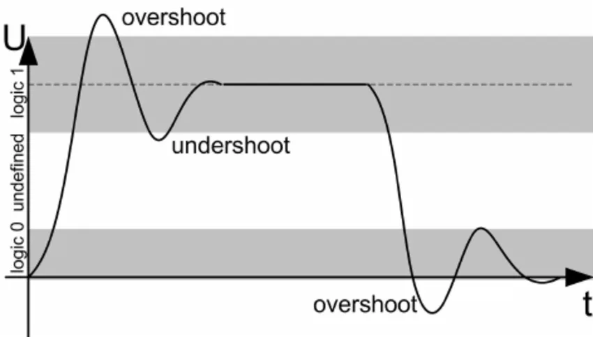
Overshoot and undershoot are potential signal integrity problems that can arise in high speed designs
Interconnect design is also related to layer stack design as your layer stack can provide shielding against EMI, determine the characteristic impedance of your traces, influence crosstalk between traces, and increase the chance your device will pass EMC tests. All these issues affect signal integrity throughout your board and whether you can implement impedance-controlled routing in your PCB.
PCB Stackup for High Speed Design
Your layer stack performs a number of functions in high-speed design and is important for signal integrity. The most popular design choice for signal integrity in multilayer boards with single-ended traces is to route them directly over a ground plane. Traces can be routed through the inner layers, but it is best to place inner signal layers between solid copper planes to prevent crosstalk and shield these traces from external EMI. Taking advantage of shielding provided by ground planes can also help you pass EMC checks.
If your board will include some analog functionality alongside high-speed digital devices, carefully segment your digital and analog sections of your board so that analog signals do not interfere with digital devices, and vice versa. You’ll also need to carefully route analog within the analog section to prevent the same signal integrity problems that can affect digital signals. Read more about designing your PCB stackup.
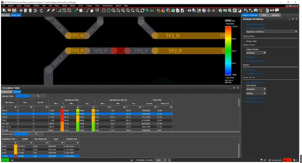
OrCAD X features signal integrity analysis tools for high speed design.
Transmission Line Effects in High Speed Signal analysis
In high speed signal analysis, when creating an impedance-matched transmission line, the key factor is the length of the interconnect between the source and the load. If the signal travel time along the trace exceeds one-quarter of the signal's rise time, the trace may behave as a transmission line. This can lead to impedance mismatches, causing signal reflections. While reflections at the source are generally ignored in high-speed design due to IC structures, reflections at the load are critical as they can cause ringing—a transient oscillation at the trace's natural frequency. A series termination resistor at the load can effectively dampen the trace and suppress ringing. For more details on transmission line effects, read about impedance-matching network design and simulation.
Preventing Clock Skew and Signal Skew in High Speed Traces
Working with high speed clocks and signals requires precise length matching of traces within some allowable tolerance. When signals are sent to a load, the signals will require some specific time to switch between ON and OFF. Traces carrying data in parallel need to be precisely length-matched to ensure that all signals reach the load at the same time. Similarly, traces with serial and parallel data streams must be length-matched to the clock signal in order to ensure that the load IC switches at the right moment. If you’d like to learn more about this subject, read about compensating skew with trace length matching.
How Parasitic Capacitance and Inductance Affect Signal Integrity
All conductive elements in a PCB have parasitic inductance, which accumulates in series and can influence signal integrity, particularly through crosstalk. While parasitics are unavoidable, their impact can be minimized by routing traces close to their reference plane or as differential pairs. In high-speed designs (10 Gbps or higher), even impedance-matched transmission lines can suffer from impedance discontinuities due to parasitics caused by variations or asymmetries in trace geometry. To combat this, traces should be length-matched and consistently spaced to maintain uniform parasitics and avoid reflections along the trace. For more information on managing parasitic capacitance and inductance, explore related resources.
Impedance Matching Network for Termination
There are a variety of termination networks that can be used to match the overall impedance of a trace to the load. This will eliminate signal reflection at the load. The best strategy is to use both strategies. Placing an appropriate series termination resistor at the load will suppress ringing by perfectly damping the trace, but this can change the value of the impedance mismatch. Placing a termination network will then ensure that the combined trace and series resistor will match the impedance at the load. If you’d like to learn more about transmission line effects, read about designing and simulating an impedance matching network.
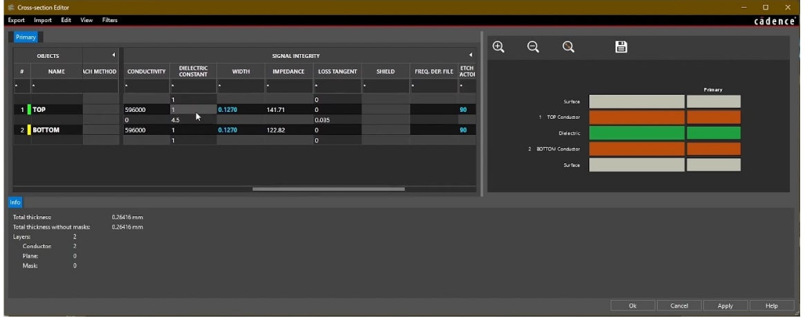
OrCAD X Cross Section Editor aids in creating stackups for high speed boards.
How OrCAD X Aids in High Speed Signal Analysis and Design
Preventing signal integrity problems in high speed design is all about having the right layout, routing, and stackup management features in your PCB design software. When coupled with signal integrity and circuit analysis tools, you’ll have everything you need to address signal integrity design considerations in high speed design.
|
Design Aspect |
How OrCAD X Aids in the Design Aspect |
|
Interconnect Design |
|
|
PCB Cross Section Editor |
|
|
Transmission Line Effects |
|
|
Clock and Signal Skew |
|
|
Parasitic Capacitance and Inductance |
|
|
Impedance Matching Network |
|
|
EMC and EMI Considerations |
|
If done properly, high-speed signal analysis will ensure that your circuits function reliably at high speeds and managing transmission line effects. Cadence’s SI/PI Analysis Point Tools provide designers with signal integrity and power integrity analysis features that are geared towards PCBs and IC packages. Learn more about how Cadence's comprehensive PCB Design and Analysis Software and OrCAD X can support your high-speed design needs.
Leading electronics providers rely on Cadence products to optimize power, space, and energy needs for a wide variety of market applications. To learn more about our innovative solutions, talk to our team of experts or subscribe to our YouTube channel.