Efficient PCB Design Validation With OrCAD X
Key Takeaways
- Incorporate validation at every stage of PCB design—from initial layout to assembly—to ensure functionality and manufacturability.
-
Use DRC in OrCAD X to catch potential design errors early, ensuring adherence to electrical and physical constraints.
-
OrCAD X supports advanced DFM and DFA checks, optimizing PCB designs for manufacturing and assembly processes.
Efficient PCB design validation involves DRC, DFM, DFA, and automated testing.
Efficient PCB Design Validation involves thoroughly assessing a circuit board design to ensure it meets its intended functionality. It is best to continuously carry it out through all stages of the PCB design process, from initial layout, to manufacturing, and assembly. This approach ensures that testing is integral to PCB design verification, ensuring the board's validation.
Efficient PCB Design Validation Steps
|
Validation Step |
Description |
|
PCB Design Rule Check |
Ensure adherence to design rules to prevent manufacturing errors. |
|
Manufacturing Capabilities through DFM |
Optimize the design for manufacturability, considering component placement and routing. |
|
Component Source and Functionality Validation |
Verify authenticity, availability, and suitability of components. |
|
Mechanical Fit, Netlist, Signal Integrity, and Thermal Analysis |
Perform checks for mechanical fit, connections, signal integrity, and heat dissipation. |
|
Gerber and Drill File Review |
Ensure accurate representation of all layers and features for manufacturing. |
|
Assembly Defects Check |
Identify and correct defects like solder balls, bridging, voids, and tombstoning. |
|
Automated Testing (ICT & Flying Probe) |
Use automated systems to validate connections and functionality efficiently. |
Efficient PCB Design Validation With DRC
Design Rule Check (DRC) is an essential part of efficient PCB design validation, as it confirms your board adheres to predefined constraints like trace width, clearances, hole sizes, and annular ring dimensions. DRC helps identify potential design errors that could lead to manufacturing defects and compromise the board's reliability. It detects both electrical and physical violations, such as power-ground shorts, misaligned vias, and missing pins.
Executing Design Rule Checks With OrCAD X
DRC supports efficient component placement and routing, ensuring that the available board space is utilized effectively. OrCAD X provides a comprehensive Constraint Manager, allowing you to set up electrical, physical, and spacing constraints, which automatically flag potential violations during the design process. Key DRC-related features include real-time clearance view and assisted routing modes, which visually highlight spacing issues and adjust traces to prevent violations. OrCAD X also supports advanced DFM (Design for Manufacturing) checks, integrating rules for fabrication, assembly, and testing, ensuring that your design is both manufacturable and reliable.
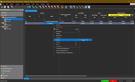
Through the constraint manager, constraint sets (CSETS) are applied to different nets or regions in the design. The image shows how to create a new CSET.
Validating Your Circuit Board for Assembly
Design for Assembly (DFA) involves a three-stage process aimed at optimizing the assembly of the board.
-
The initial stage focuses on the board layout, where considerations such as component spacing, soldering direction, and cost-effective assembly strategies are addressed.
-
The next stage involves validating Gerber or ODB++ files to ensure proper clearances, component orientations, and footprint accuracy, as well as assessing the effectiveness of cleaning methods
-
The final stage identifies the specific soldering techniques required, including wave soldering, reflow soldering, and manual soldering, to ensure a smooth assembly process.
Circuit Board Assembly Validation With OrCAD X
OrCAD X provides advanced features that allow designers to define precise package-to-package spacing rules, ensuring components are properly spaced for automated assembly processes. Additionally, the ability to categorize components into groups like chip parts, ICs, and connectors allows for applying tailored spacing rules across different PCB regions, enhancing the overall assembly efficiency.
Component Source Validation
Carefully validating each component's source is important to ensure authenticity of parts and prevent issues like delays, misinformation, and the risk of counterfeit components. As part of efficient PCB design validation, it's essential to ensure all components listed in the BOM are readily available and not obsolete or nearing end-of-life status. Utilizing an intelligent BOM software is the best way of doing this.
Ensuring component sourcing through OrCAD X is streamlined with Live BOM. The Live BOM feature in OrCAD X allows designers to integrate real-time component data directly into their design environment, making it easy to check component availability, pricing, and lead times as the design progresses. This feature connects to supplier databases, providing instant access to the latest information on component sourcing, helping designers avoid supply chain issues and ensuring that the components selected for the design are both available and cost-effective. The Live BOM feature also supports automatic updates, ensuring that any changes in component status are immediately reflected in the BOM.
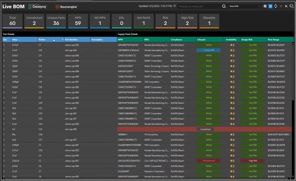
OrCAD X Live BOM provides compliance lifecycle, status, market availability, and price
Post Assembly PCB Validation Tips
Post assembly, there are two primary methods for validation:
-
In-Circuit Testing (ICT) uses a custom fixture with precisely placed probes to test each board. Typically, the fixture’s probes make contact with test points on the board. Due to their complexity and cost, ICT fixtures are usually reserved for mass production of well-established designs, making them ideal for quickly testing large quantities of boards.
-
Flying Probe Testing uses a small number of probes that move around the board, testing each net sequentially. Although slower and unable to perform functional testing due to the lack of simultaneous connections, flying probe systems are cost-effective and flexible.
Assembly defects:
-
Solder Balls: These are tiny spherical particles of solder that separate from the main joint during assembly. In a no-clean process, multiple solder balls can form bridges between adjacent leads, causing operational problems.
-
Solder Bridging arises when solder unintentionally connects two conductors that should remain electrically separate, leading to shorts.
-
Solder Voids: These are empty spaces or holes within a solder joint, often consisting of air, which occur when insufficient solder is present to make a proper connection.
-
Tombstoning (Manhattan Effect) occurs when an SMD component is partially or entirely lifted off its landing pad. It's most common in small SMD passives (0603 or smaller packages) and typically results from force imbalances during reflow soldering.
The Role of OrCAD X In Validating PCB Fabrication and Assemblies
In OrCAD X, DFF constraints focus on the PCB layer fabrication, including mask, copper, and silkscreen layers. This includes checks like copper spacing, outline checks, and maximum line width to pad ratio, which help prevent issues like shorts, solder bridging, and other fabrication-related defects.
On the other hand, DFA constraints focus on the assembly process, addressing issues such as component placement and spacing. This includes rules like package-to-package spacing, via under component checks, and through-hole pins under SMD components, ensuring that the board can be assembled without errors like tombstoning or solder voids. These checks are highly configurable, allowing designers to set specific rules for different regions of the board or for different types of components, optimizing the design for the actual manufacturing and assembly processes-.
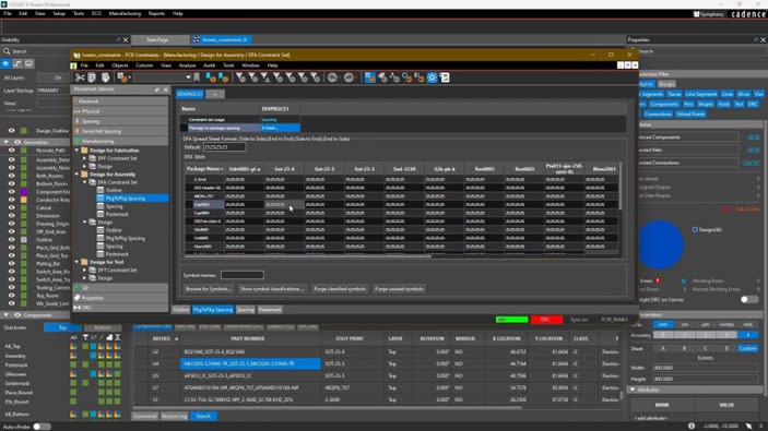
Setting up package-to-package spacing DFA rules
Efficient PCB design validation involves ensuring your board meets all necessary requirements from design to assembly. OrCAD X offers powerful features to assist designers in achieving efficient PCB design validation through advanced DRC, DFM, and DFA checks. To learn more about how Cadence tools can enhance your PCB design process, visit our PCB Design and Analysis Software page and explore OrCAD X.
Leading electronics providers rely on Cadence products to optimize power, space, and energy needs for a wide variety of market applications. To learn more about our innovative solutions, talk to our team of experts or subscribe to our YouTube channel.