PCB Design and Analysis Hub

Tutorials, Workflows, and Engineering Insights for Reliable PCB Design

FEATURED CONTENT

Stay Informed on the Latest PCB Updates

6 results found

LATEST BLOG, DESIGN GUIDE, EBOOKS & MANY MORE

Design Insights Across the PCB Lifecycle

Sample content thumbnail
AI in PCB Design: What Works Today and What Doesn’t
AI in PCB design: learn which AI tools deliver real results today, where limitations remain, and how engineers can use them effectively.
View Now
Sample content thumbnail
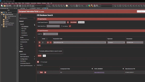
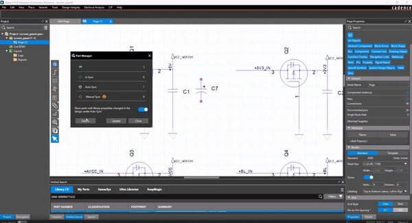
How to Place Parts from a Component Database in OrCAD X CIP
Learn how to place verified parts from your component database in OrCAD X Capture CIS using OrCAD X CIP parametric search and browsing workflows.
View Now
Sample content thumbnail
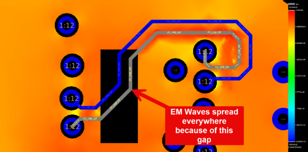
Why DDR and PCIe Cause EMI and How to Stop It
Why do your DRCs pass but your board fails EMC? Stop guessing. Learn how fast edge rates and layout errors turn your DDR and PCIe designs into antennas, and how to spot-check EMI before fabrication.
View Now
Sample content thumbnail
Evaluating EMI Risk in PCB Design Before Hardware Testing
Catch EMI risks before hardware testing. Learn a four-step pre-tapeout workflow to reduce PCB respins by finding return path, PDN, and mode conversion issues in your routed layout.
View Now
Sample content thumbnail
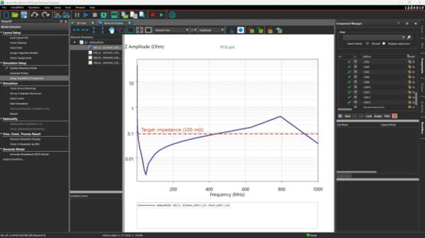
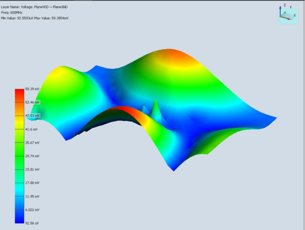
Power Distribution Noise and Its Impact on EMI in PCB Design
Power distribution noise becomes EMI through plane resonance, reference ripple, and ground bounce. Learn the three layout decisions that break the chain.
View Now
Sample content thumbnail
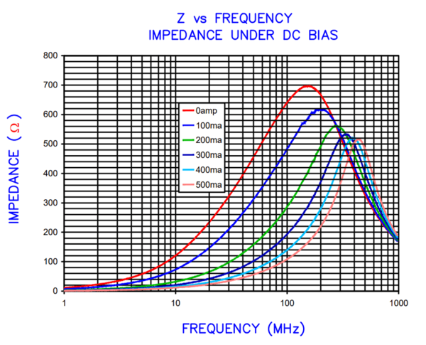
When Do Ferrite Beads Help or Hurt EMI Performance in PCB Designs?
Ferrite beads can reduce EMI, but the wrong placement can cause resonance, hurt power integrity, or shift noise.
View Now
6 results found

VIDEOS

Power Up PCB Projects With Design Solutions and Innovations

Top 5 Reasons your Vias Cause your High Speed Signals to Fail
Your traces look good. Your connections look perfect. But your high speed board still fails channel analysis. In this video, EE design consultant Kirsch Mackey counts down the top 5 via mistakes that quietly wreck high speed signals, and shows you exactly how to fix each one. Vias aren't just vertical connections through the board. At high speeds and short rise times, they're discontinuities for the electromagnetic wave. Manage them wrong, and your channel signals can fail even when the layout looks flawless. In this video: 00:00 – Intro: why vias fail even when everything else looks right 00:25 – Mistake #5: Bad antipad geometry 00:51 – Mistake #4: Using the wrong via type for your data rate 02:05 – Mistake #3: Ignoring via stub resonance 03:02 – Mistake #2: Asymmetric differential pair vias 03:54 – Mistake #1: Signal vias without a return via 05:15 – Key takeaway
Watch Video
Sample content thumbnail
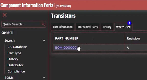
How to Use “Where Used” Functionality in OrCAD X CIP for Obsolescence and BOM Risk Analysis
Learn how to use Where Used functionality in OrCAD X CIP to identify affected designs, analyze obsolete components, reduce BOM risk, and streamline component replacement across PCB projects.
Watch Video
Sample content thumbnail
CIP for System Capture: Centralized Component Management, NPI, and Supply Chain Intelligence
Use CIP within Allegro X System Capture to centralize component data, streamline new part introduction, assign alternates, track part usage, and leverage real-time supply chain intelligence.
Watch Video
Sample content thumbnail
How to Identify Where Obsolete Components Are Used with OrCAD X CIP
Quickly identify where obsolete components are used across PCB designs with OrCAD X CIP. Perform where-used analysis, reduce redesign risk, and improve component lifecycle management.
Watch Video
Sample content thumbnail
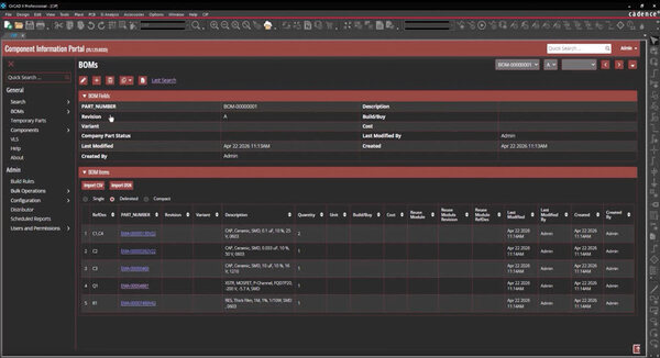
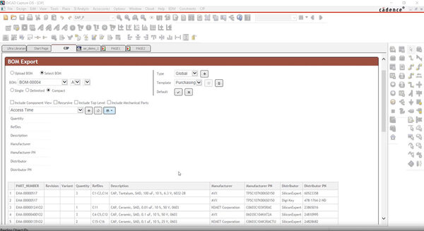
Real-Time BOM Intelligence for PCB Design with OrCAD X CIP Compliance Module
Integrate real-time BOM intelligence into PCB design with OrCAD X CIP. Analyze component lifecycle, compliance, availability, and sourcing risk to reduce redesigns and improve manufacturability.
Watch Video
Sample content thumbnail
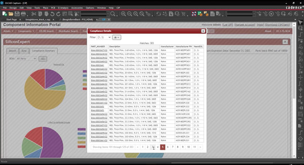
How to Analyze PCB Component Compliance Risk in OrCAD X CIP
Analyze lifecycle, sourcing, and compliance risk across your PCB component database in OrCAD X CIP. Assess BOM exposure and make resilient decisions with real-time supply intelligence.
Watch Video
6 results found

Resources

Deep Dive Into PCB Engineering Content

Sample icon

Navigate complex PCB design challenges with in-depth guides including practical advice, and proven techniques.

Sample icon

A comprehensive set of inline documentation for OrCAD X PCB Designer covering theory, workflow, and configuration options.

Sample icon

Dive deep into PCB design and analysis with comprehensive technical papers, whitepapers, datasheets, and infographics.

Try OrCAD X today

Experience the Power of OrCAD X for PCB Design

An essential routing, real-time collaboration, integrated signal integrity analysis, and constraint-consistent manager — start designing in minutes.

Download the free tool

Scale up with Allegro X

Faster design cycles, enhanced collaboration, and seamless integration across an enterprise workflow for comprehensive system design.