DDR Timing Constraints With Allegro X
Key Takeaways
-
Trace Length Matching: Critical for timing alignment, with a common tolerance of ±10 mils to prevent data corruption and operational failure.
-
Impedance Control: Maintain consistent impedance (50Ω single-ended, 90Ω differential pairs) to avoid signal reflections and loss.
-
DDR Routing Tools: Allegro X provides advanced features like Auto Delay Tune and Timing Vision for effective DDR routing and constraint management.
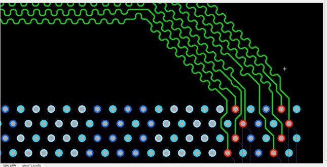
Allegro PCB Designer automatically create serpentine traces to ensure adherence to DDR timing constraints.
DDR routing must adhere to design guidelines that address inherent electrical challenges to maintain signal integrity and functionality. Designing with DDR timing constraints in the forefront of the designer's mind is critical for eliminating static and ensuring high functionality. This is where applying constraints, or design rules, into the DDR routing design comes in handy.
Common DDR Timing Constraints for PCB Design
|
Constraint |
Typical Values / Guidelines |
Description & Notes |
|
Operating Temperature |
Commercial-grade: 0°C to 85°C Industrial-grade: -40°C to 105°C |
- Defines the temperature range within which DDR memory components can operate reliably. - Ensure that the PCB design and thermal management solutions account for the operating temperature range of the DDR components to avoid thermal-induced failures. |
|
Trace Length Matching |
±10 mils (0.25mm) between data, strobe (DQS), and clock (CK) traces. |
- Ensures that the lengths of all data, address, control, and clock traces are matched to within a specified tolerance to avoid timing skew. - Proper length matching is crucial for timing alignment. - Length discrepancies can lead to timing issues, causing data corruption or operational failure. - Serpentine routing may be necessary to achieve length matching. |
|
Trace Spacing |
Differential pairs: 5 mils (0.127mm) spacing within the pair, 20 mils (0.508mm) to other signals. |
- Maintains consistent spacing between differential pairs and other signals to avoid crosstalk and skew. |
|
Impedance Control |
Single-ended: 50Ω ± 10% . |
- Maintains consistent impedance across all DDR traces to prevent signal reflections and loss. |
|
Differential Pair Routing |
Pair spacing: 3 to 5 mils (0.0762mm to 0.127mm) |
- For differential signals like DDR clock (CK) and data strobe (DQS), traces should be routed as tightly coupled pairs. |
|
Trace Angles |
Minimum angle: 45° |
- Acute angles (less than 45°) can cause signal reflections and impedance discontinuities, degrading signal integrity. |
|
Via Usage |
0-1 via per trace (ideally zero for clock and strobe lines) |
- Minimize the use of vias on DDR signals to reduce inductance and maintain signal integrity. |
|
Stub Length |
Maximum stub length: ≤ 5 mils (0.127mm) |
- Reduce or eliminate stubs (unconnected trace lengths) to avoid reflections and signal degradation. |
|
Termination |
Series termination: 22Ω to 33Ω resistors placed close to the source. |
- Series termination is often used to match the driver’s impedance with the trace impedance, reducing reflections. |
|
Supply Voltages |
DDR3: 1.5V ± 0.075V |
- Power integrity analysis is recommended to ensure stable voltage levels. |
|
Setup and Hold Times |
DDR3: Setup time: 100ps |
- The minimum time before and after the clock edge that data must be stable. |
|
Cross Talk |
Signal line spacing: 3x to 5x the trace width. |
- Ensure adequate spacing between signal lines to minimize crosstalk, which can cause data errors. |
|
Timing Skew |
DDR3: ≤ 25ps between data lines within a byte lane. |
- The allowable difference in timing between related signals, particularly between data lines and the clock. - Skew can be controlled by ensuring matched trace lengths, proper spacing, and controlled impedance routing. |
|
Clock Trace Routing |
Minimize clock trace length and match it closely with other clock-related signals. |
- Route clock lines with minimal delay and jitter, and ensure they have the shortest and most direct path possible. |
|
Via Stub Length (for high-speed signals) |
Backdrill vias to remove stubs: ideally, stub length should be ≤ 10% of the signal wavelength at DDR frequency. |
- Reduce the length of via stubs to avoid resonant frequencies that can degrade signal quality. |
What are DDRs?
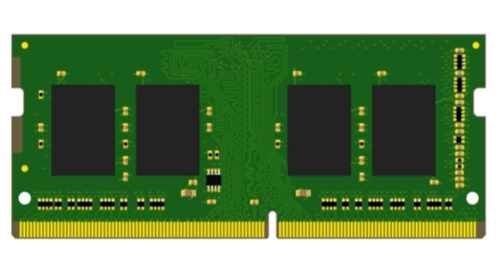
Printed circuit board (PCB) layouts often use some form of Double-Data Rate (DDR) memory. As the name suggests, DDR memory allows TWO data bit transitions to occur during a single clock cycle, thereby doubling the data capacity during a single cycle. The term, "double data rate" means that it can fetch data on both the up and the down cycles of the timing clock, unlike the previous versions of RAM which only fetched on one clock edge. With DDR timing constraints in mind, memory devices are often hand-routed to maintain thoughtful control over potential routing issues, such as proper separation between address, data, and control signals.
DDR routing is becoming more and more widespread through electronics design.
Constraints for DDR Routing
The increased speed of DDR memory circuits has rendered the PCB layout more complex. Timing and signal integrity are critical at high speeds with large data transfers. Designers employ a prescribed set of "constraints" -- to be utilized in the DDR routing layout. Constraints in DDR routing can include elements such as delayed timing and matched lengths, and temperature limits imposed by surrounding components.
DDR routing constraints can feel restricting and demanding to the designer, sure, but consider this: some very bright minds ahead of you have created those constraints in DDR routing to make your job easier and your PCB functionally successful the first time.
Constraints in DDR routing may involve:
- Operating temperature: DDR memory components typically operate within a temperature range of 0°C to 85°C for commercial-grade components and -40°C to 105°C for industrial-grade components.
- Common Trace angles, length, and distance between traces
- Trace Length Matching: The length of the data, strobe (DQS), and clock (CK) traces should be matched within a tolerance of ±10 mils (0.25 mm) to ensure proper timing.
- Trace Spacing: Differential pairs (e.g., DQ and DQS) should maintain a consistent spacing to avoid skew, typically 5 mils (0.127 mm) between the traces within the pair, and 20 mils (0.508 mm) to other signals.
- Trace Angles: Avoid acute angles (less than 45°) in trace routing to prevent signal reflections and maintain signal integrity.
- Termination: For DDR3/DDR4, series termination resistors (e.g., 22Ω to 33Ω) are often placed close to the controller or memory device to match the impedance of the traces (typically 50Ω).
- Supply voltages: DDR3 operates at a nominal supply voltage of 1.5V (±0.075V), while DDR4 operates at 1.2V (±0.06V). It's essential to maintain these voltages within the specified tolerances to avoid operational failures.
- Setup and hold times: Setup time is the minimum time before the clock edge that the data must be stable, while hold time is the minimum time after the clock edge that the data must remain stable. For DDR3, typical setup and hold times are 100ps and 50ps, respectively.
- Impedance Control: The differential pair impedance for DDR3/DDR4 should be maintained at 90Ω ±10%. Single-ended traces should be controlled to 50Ω ±10% to match the characteristic impedance of the PCB stack-up.
- Timing Skew: The timing skew between the clock and data lines should be minimized. For DDR3, the acceptable skew between data lines within a byte lane is typically 25ps or less.
Failure to follow recommended constraints in DDR routing will produce circuits that do not perform as intended and will function erratically. Difficult to troubleshoot, memory circuits can malfunction so minutely that data corruption can be seen only when particular data streams are passed in and out, or at specific operating temperatures.
Adding bumps to the trace to resolve a timing delay in Allegro PCB Designer.
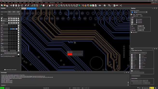
Adherence to DDR Timing Constraints With Allegro X
The never-ending drive towards miniaturization has increased the incidence of designs where analog, digital, and RF circuits are closely combined with high voltage circuits. These high voltage circuits require additional constraints in DDR routing in the form of increased electrical clearances and isolation for operator safety.
Allegro X Features for DDR Routing
|
Feature Name |
What It Does |
How It Aids in DDR Routing Constraints |
|
Allegro Timing Environment |
Manages timing constraints and tuning within the PCB design environment. |
Provides a centralized environment to manage and optimize DDR signal timing, ensuring all timing constraints are met. |
|
Auto Delay Tune |
Automatically adjusts trace lengths to meet delay requirements using methods like accordion, sawtooth, and trombone. |
Ensures that all traces meet length matching requirements, critical for maintaining signal timing and integrity in DDR routing. |
|
Auto Phase Tune |
Automatically adjusts the phase of differential pairs to maintain phase alignment within required tolerances. |
Minimizes phase skew between differential pairs, which is essential for reliable data transmission in DDR interfaces. |
|
Remove Tuning |
Removes previously applied delay or phase tuning adjustments. . |
Allows designers to revert tuning changes if necessary, maintaining the integrity and accuracy of DDR routing. |
|
Min/Max Propagation Delay |
Sets specific minimum and maximum propagation delay constraints for signals. |
Ensures consistent delay characteristics across DDR signals, crucial for maintaining timing margins and avoiding data errors. |
|
Timing Vision |
Provides real-time visual feedback on the timing status of routed signals, using color-coded indicators. |
Helps quickly identify and correct timing issues, ensuring that all DDR signals are synchronized and within constraints. |
|
Pin Delay and Z-Axis Length Calculation |
Includes pin and via (Z-axis) delays in signal length calculation |
Provides a more accurate assessment of total signal delays, ensuring DDR timing constraints are met across all signal paths. |
|
Advanced Constraint Formulas |
Allows the creation of complex length and timing relationships between nets using formulas. |
Enforces specific timing relationships, such as matched lengths or timing ratios, essential for DDR routing |
|
Physical Constraints |
Defines physical rules like track width, necking, and via types, ensuring proper impedance and signal integrity. |
Maintains the required electrical characteristics of DDR signals, ensuring they perform correctly under all operating conditions. |
|
Relative Propagation Delay (Match Groups) |
Groups signals for matched length tuning within specified tolerances. |
Ensures that all signals in a DDR bus or interface are length-matched, preventing timing mismatches and signal integrity issues. |
Cadence's Allegro PCB Designer is a scalable design tool that contains everything needed to create a PCB layout with a fully integrated design flow. The heart of Allegro PCB Designer contains a constraint management system, PCB Editor, for creation, management, and validation of constraints in DDR routing. It also includes an auto-interactive router, and interfaces for design for manufacturability (DfM).
Mastering DDR timing constraints is important for high-speed memory designs. Cadence's tools, including Allegro X, are designed to help you seamlessly implement these constraints into your PCB designs. Explore more about how Allegro X can streamline your design process by visiting our PCB Design and Analysis Software page and learning about Allegro X.
Leading electronics providers rely on Cadence products to optimize power, space, and energy needs for a wide variety of market applications. To learn more about our innovative solutions, talk to our team of experts or subscribe to our YouTube channel.