OrCAD X Library Footprint Path and Information
Key Takeaways
-
Properly configuring library footprint paths in OrCAD X ensures accurate netlisting
-
The footprint editor in OrCAD X allows direct modification and updating of footprints
-
OrCAD X includes a footprint generator to automate the creation of industry-standard footprint packages
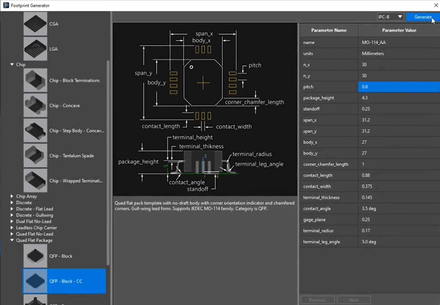
OrCAD X Footprint Generator
Configuring an OrCAD X library footprint path makes it easy to ensure that schematic symbols link properly to their corresponding PCB footprints. In OrCAD X, footprint libraries are stored in designated directories, and configuring these paths correctly helps prevent errors during netlisting and layout. Understanding how to manage, edit, and automate footprint generation within OrCAD X can streamline your PCB design workflow and improve accuracy. This guide will discuss it all.
Configuring OrCAD X Library Footprint Paths
One of the critical steps in managing your PCB designs is ensuring that your schematic symbols correctly link to the corresponding PCB footprints. In OrCAD X, footprint libraries are stored in specific directories – for example, many systems use paths such as:
C:\Cadence\SPB_<version>\share\pcb\pcb_lib\symbols.
When you add a schematic symbol to your design, it’s essential to set the correct footprint path so that during netlisting the tool locates the right physical representation.
Managing and Editing Footprint Libraries in OrCAD X Workflows
OrCAD X not only allows you to configure library paths but also offers workflows for editing footprint data.
-
Right-click the component in your layout and select “Edit Footprint”.
-
If the footprint exists in your library, it opens automatically; if not, you’ll be prompted to export it to your working directory.
-
The Footprint Editor window opens alongside your original layout database.
-
Make your edits (e.g., move pins, add pins, modify pad stacks) as needed.
-
When finished, choose Exit from the file menu and save your changes.
-
Back in the layout editor, you’ll be prompted to apply the updates—confirm to refresh all instances of that footprint in your design.
How the Component Information System (CIS) in OrCAD X Aids in Library Footprint Organization
CIS integrates a centralized part database directly into the OrCAD X Capture environment, enabling you to instantly review symbols, footprints, parametric details, and supply chain information—all in one place.
OrCAD X library footprint paths are integrated into the Component Information System (CIS), ensuring that schematic symbols are automatically linked to their correct PCB footprints. This centralized approach simplifies footprint management across your design environment by allowing direct review and updates through the integrated part database.
OrCAD X Template Driven Footprint Creation
Creating accurate PCB footprints is important, especially if you are using uncommon components. OrCAD X significantly simplifies this process by automating the creation of hundreds of industry-standard footprint packages. Designers can select the type of footprint they need, fill in the specific parameters tailored to their design requirements, and then specify the relevant IPC class to ensure compliance. Once these inputs are provided, the software generates a complete footprint that includes all essential elements—such as keepouts, pins, and solder masks—while also producing an integrated 3D model of the package.
This streamlined, automated process not only saves valuable design time but also enhances accuracy and manufacturability across the entire PCB design workflow.
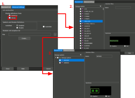
Locating and Browsing Included PCB Footprint Libraries in OrCAD X
Many designs require manufacturer-specific or standardized footprints (e.g., SOIC, DIP). OrCAD X includes pre-built footprint libraries to jump-start your design process.
|
Step |
Instruction |
Details |
|
Access via File Explorer |
Navigate to the footprint libraries folder |
Open File Explorer, go to the main *C:* drive, and then browse to: C:\Cadence\SPB_[version]\share\pcb\pcb_lib\symbols |
|
Open OrCAD X |
Launch the tool and access components |
Start OrCAD X Presto and select Place > Components Manually to open the Placement window. |
|
Enable Library Display |
Activate advanced settings |
In the Placement window, click on the Advanced Settings tab and check Library under “Display Definitions From.” |
|
View Package Symbols |
Populate the list of footprints |
Return to the Placement List tab and select Package Symbols from the dropdown to display available footprint entries. |
|
Preview and Search |
Verify and locate specific footprints |
Select an entry to preview the footprint. To search, type a footprint name into the Match field under Selection Filters. Use wildcards (e.g., *0402* or SM?0402) for broader or refined searches. |
New Footprint Library Capabilities in OrCAD X 24.1
OrCAD X introduces a powerful footprint generator accessible under File > New Template Based Footprint, offering a library of ITC-based footprint templates. The generator provides detailed parametric controls for creating precise PCB footprints across multiple component categories.
OrCAD X Footprint Generator Features
|
Key Technical Features |
Details |
|
Component Types |
- Area arrays - Shift arrays - Discrete components - Lead components - Peripheral components - Through-hole and surface mount variants |
|
Parametric Generation Controls |
Designers can customize: - Number of pins in X and Y directions - X and Y pitch - Package height - Standoff dimensions - Terminal diameter - IPC compliance levels (A, B, C) |
|
Automatic Generation Capabilities |
- Automatic pad stack creation - Component boundary generation - Keepout and keepin zone definition - Integrated 3D model generation - Real-time parameter modification - Instant regeneration of footprints |
|
Advanced Workflow Benefits |
- Hundreds of parametric footprint templates - Graphical parameter visualization - Rapid design iteration - Reduced manual footprint creation time - Minimized human error potential |
Configuring your OrCAD X library footprint paths correctly is essential for accurate PCB design and layout. OrCAD X provides a streamlined solution for footprint management, editing, and automated generation, reducing design errors and improving efficiency. Learn more about OrCAD X and try out a free OrCAD X trial.
Leading electronics providers rely on Cadence products to optimize power, space, and energy needs for a wide variety of market applications. To learn more about our innovative solutions, subscribe to our newsletter or our YouTube channel.