02 - Creating a PCB Layout in OrCAD X Presto - Basic Design Tasks
The OrCAD X Presto design environment enhances the productivity of layout designers and accelerates the layout design process. Its intuitive and efficient features accelerate the overall PCB design turnaround time and reduce time to market.
To create a PCB layout in OrCAD X Presto, you need to complete the design tasks in the dropdown menu below.
Creating a New Board Design
Layout design begins with creating a new board design. To do so, follow these steps:
- Choose Start – Cadence PCB 2023 – OrCAD X Presto 2023 on Windows.
The Cadence Product Choices dialog box is displayed.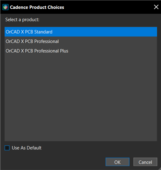
- Choose a product license and click OK. OrCAD X Presto is launched, and the Start Page is displayed.
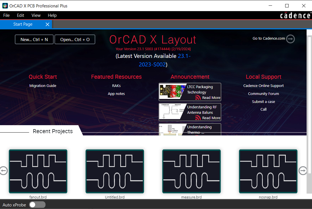
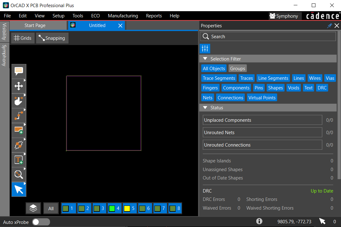
- Choose File – New – Board to create a new board design (.brd) file. A blank board (Untitled.brd) with a default rectangular design outline opens in a new tab.
- Choose File – Save As to specify the name and path of the board design.
The design name shows in the tab. A tooltip displays the path when you hover the cursor over the tab.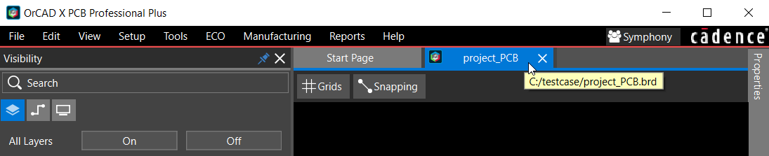
Configuring Component Footprint Libraries
After creating a blank layout (.brd) in OrCAD X Presto, you need to define the path of footprint libraries. A footprint library is a collection of graphic symbols representing packages (.*sm), mechanical elements, drawing formats (.dra), and custom pads and padstacks (.pad). To specify the path of component footprint libraries, do the following:
- Choose Edit – Preferences to open the Preferences dialog box.
- In the left pane of the dialog box, select the Directories & Paths folder under Libraries.
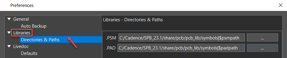
- To define the path to package symbols (footprints), click the browse button for the Footprint
.PSM search pathfield.
The psmpath Items dialog box is displayed. - To add a library path, click the
 icon.
icon. 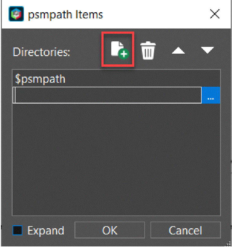 An empty item is added to the list.
 - Click the browse button next to the newly added item. The Select Directory dialog box opens.
- Navigate to the location of the footprints library directory and click OK.
- Click the up arrow button to set the path to the footprint library before the default library.
If there are common components in both the libraries, the library that appears first in the list is honored.
- Click OK to close the psmpath Items dialog box.
- Repeat steps 1 - 8 for the Padstacks.PAD search path field to specify the path of the padstack library.
- Click OK to close the Preferences dialog box.
Setting Up Layers Stack-Up
When creating the layer stack-up, it is necessary to define the various characteristics of PCB layers, including their material, layer type, name, thickness, dielectric constant, and electrical conductivity. While routing, you might need to insert additional routing layers because the design is too dense to complete or delete extra layers because of an ECO.
OrCAD X Presto provides a spreadsheet-based utility, Cross-section Editor to specify an accurate layer stack-up. You can view and modify the board layer setup in the Cross-section Editor window by adding or deleting layers.
Add or modify layers as follows:
- Choose Tools – Cross Section.
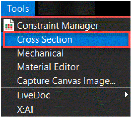 The Cross-section Editor window opens. The spreadsheet rows represent the primary layer material (stack-up), and the columns represent the various properties of each layer (conductor and dielectric). The rows are displayed in the physical order, starting from the TOP layer and ending at the BOTTOM layer.
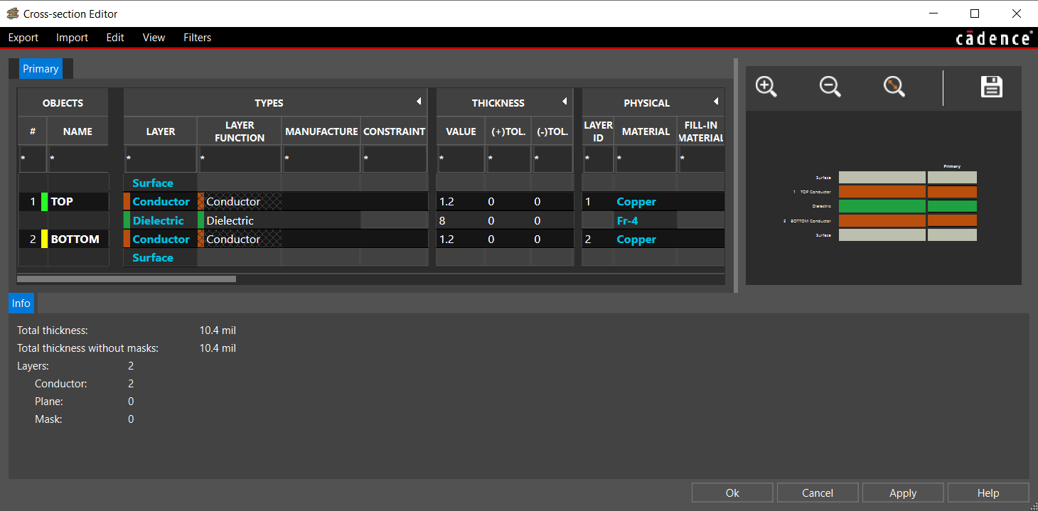
- To add a new layer, right-click a layer in the Primary tab and choose Add Layer Above or Add Layer Below. The Add Layers dialog box opens.
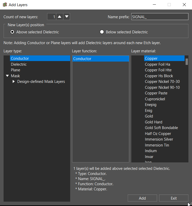
- Specify the number of layers to be added, prefix for layer name, position of the new layers, layer type, layer function, and layer material, and click Add in the Add Layers dialog box. New layers are added above or below the selected layer.
- Click Exit to close the Add Layers dialog box.
- Optionally, choose Add Layer Pair Above or Add Layer Pair Below to add a pair of layers.
- To change a layer definition, do the following steps in the Object column:
- Select the Layer Name cell and specify a name for the layer.
- In the Layer Function column, specify the layer type to define the purpose that layer serves in the layout design. For example, Signal.
- In the Material column, choose a material type from the list to define the electrical characteristics of the layer provided by the manufacturing partner. For example, Copper.
- In the Thickness column of the layer, enter a number representing the thickness for that layer. The thicknesses of an individual layer can be derived from the manufacturing data supplied by the manufacturing partner.
- In the Conductivity column, enter the value of the electrical conductivity of the layer as provided with the manufacturing specifications.
<installation_directory>\latest\share\pcb\text
The default settings for the Cross-section Editor window are stored and maintained in the materials.dat file that exists in the following location:
- Repeat steps 1 - 6 to add more layers to the board.
- Select the layer, right-click, and choose Remove Layer delete a layer from the cross-section.
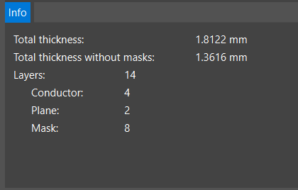
- View the cross-sectional summary of a board design in the Info tab at the bottom of the Cross-section Editor window. This Info tab displays the total number of layers of each type and their thickness.
- Close the Cross-section Editor window when you have finished setting up layers.
Placing Components
To place components in a design in OrCAD X Presto, do the following:
- Choose ECO – Quickplace Components to place all the components in the design canvas in a single step.
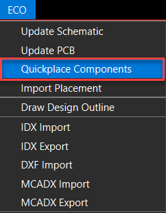 All components are placed along the longest edge of the design outline shape. Rats are displayed between pins of the same net and help you place connected components close to each other.
 - Click the Move icon
 from the functional toolbar to move symbols inside the design outline. The selected symbol attaches to the cursor.
 - Optionally, in the Arrange pane of the Properties panel, click the Rotate Left or Rotate Right
- button to rotate the symbol by 90 degrees either clockwise or counterclockwise.
- Check the Status pane for Unplaced Components in the Properties panel to verify that all the components are placed.
Routing the Board
![]() OrCAD X Presto provides various options to route connections on a board. Route a net as follows:
OrCAD X Presto provides various options to route connections on a board. Route a net as follows:
- Click the Add Connecticon from the functional toolbar. The route widget opens, displaying options for routing single connect lines (traces) and differential pairs.
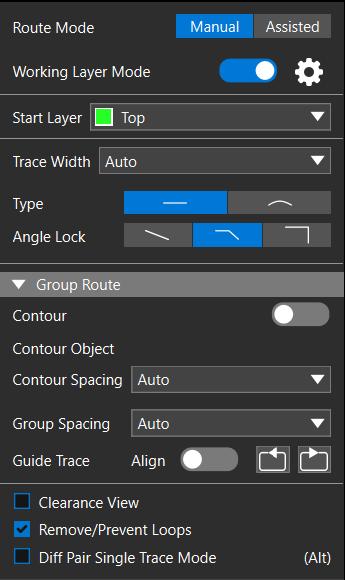
- Set Route Mode to Manual.
- Set Trace Width to Constraint. The default width of the connect line is defined in Constraint Manager.
- Choose a net to route and move the cursor to start routing.
- To route the trace on a different layer, double-click to insert a via.
- To adjust the route, click the Slide
 icon from the functional toolbar. The slide widget displays options to slide the traces.
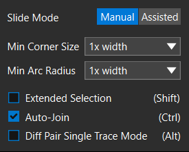
- Set the Slide Mode to Manual.
- Route all of the nets in the design.
- Click the zoom fit icon
 from the functional toolbar to view the complete design.
Documenting PCB Design
Once the layout design is completed and checked for errors, the documentation phase begins, which includes the creation of fabrication and assembly drawings, generation of drill data, artwork, and so on. OrCAD X Presto offers LiveDoc, which automates the documentation process using predefined templates to quickly capture the manufacturing and assembly requirements.
Exporting Design Data
The Exports dialog box generates manufacturing output (fabrication and assembly data). You can se- lect multiple manufacturing output formats and generate all the data as an archived file in a single step.
To generate output files, follow these steps:
- Choose Manufacturing – Export to Manufacturing. The Exports dialog box opens. Default manufacturing output formats are listed on the left, while settings are displayed on the right.
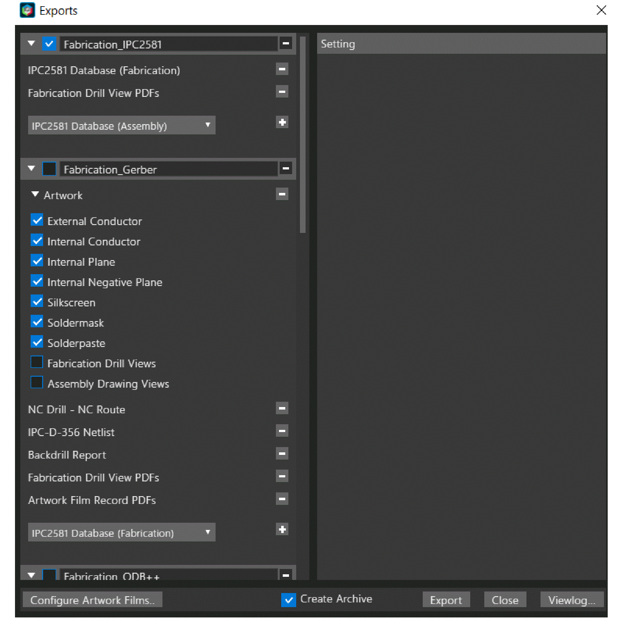
- To select a manufacturing output, enable the check box before it. By default, Fabrica- tion_IPC2581 is selected.
An installation of ODB++ Inside the software package is required to generate output files for Fabrication_ODB++.
- To generate a manufacturing data format, choose it from the list and click the
 icon.
icon. 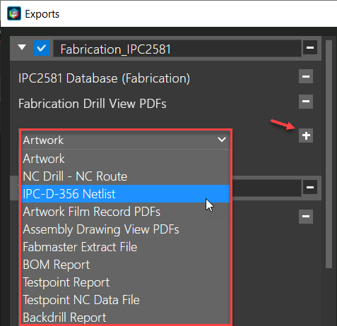
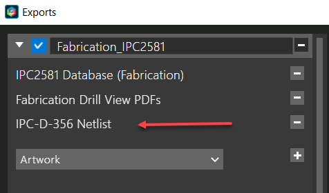
- Click
 to remove a manufacturing data format you do not want to generate.
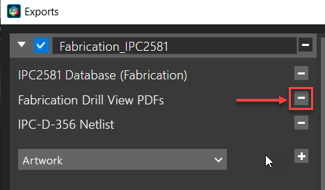
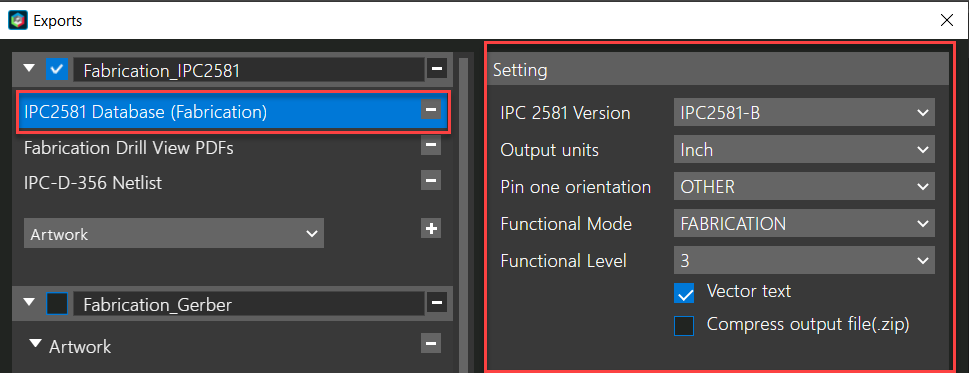
- To modify the parameters of a manufacturing data format, choose it in the left section and change the values in the Setting section displayed on the right.
- Select the Config File pull-down field to save the export configuration as a .json file. The default export configuration file exists
- Select the Archive check box.
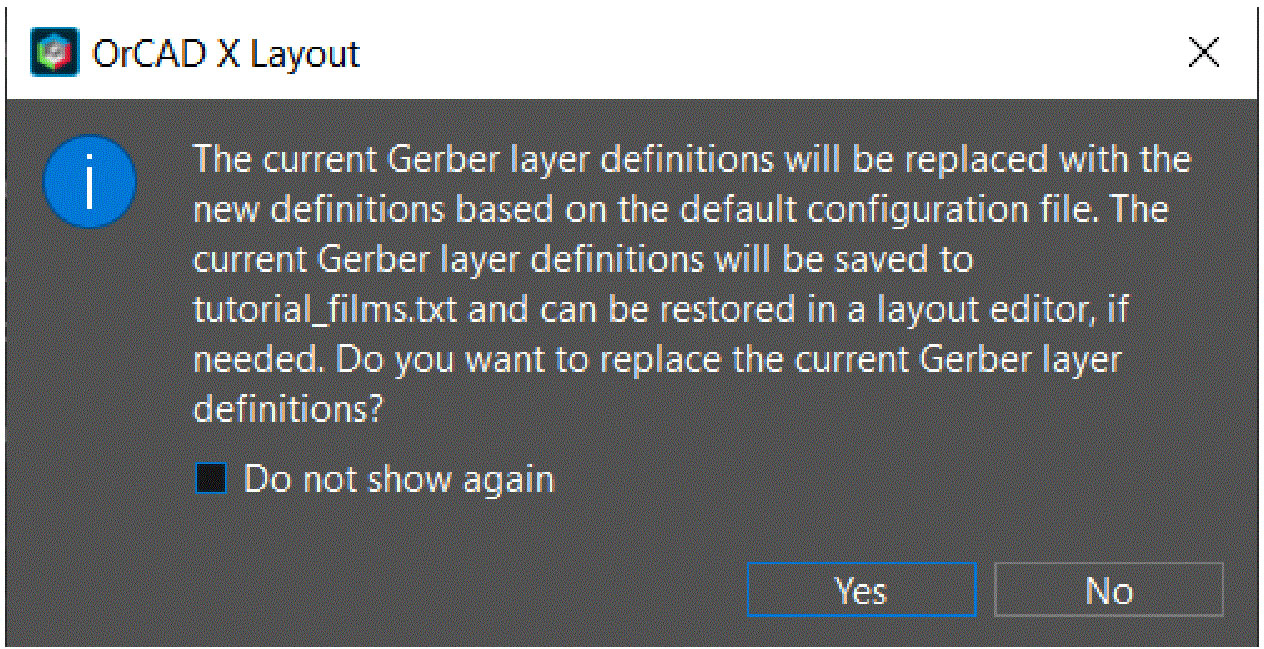
- Click Export to generate all the selected manufacturing outputs as archived files.
- Click Yes in the following message prompt.
 A progress bar displays the status of the export process.
 - Click Viewlog to open the log file and review the errors and warnings.
View the next document: 03 - Authoring and Editing Footprints in OrCAD X Presto
If you have any questions or comments about the OrCAD X platform, click on the link below.
Contact Us