02 - Simulating a Design
In this section, you will use PSpice to simulate the design created in the previous section using Capture CIS. You will also learn about transient analysis that is performed using PSpice.
Getting the Design Ready for Simulation
To simulate a design, the PSpice simulator needs information about circuit topology, analysis type, and stimulus definitions.
The analysis type, stimulus definition, and the information related to the initial digital state of the simulation is provided by a simulation profile (*.SIM). In the following section, you will create a simulation profile.
Creating a Stimulus File
Before creating the simulation profile, you need to specify the stimulus definition to be used for simulating the circuit. For this, you need to create a stimulus file and then specify its location in the Simulation Setting dialog box to create the simulation profile.
- To create the stimulus file, copy the following information in a text editor (.txt) file and save it as stimulus.stl.
.STIMULUS IN_HIGH STIM (1, 1)
+ 0 0
+ +0 1
.STIMULUS S_SI STIM (1, 1)
+0ms 0
+808.400000000u 0
+ +200ns 0
+ +200ns 0
+ +200ns 0
+ +200ns 0
+ +200ns 1
+ +200ns 1
+ +200ns 1
+ +200ns 0
+ +200ns 0
+ +200ns 0
+ +200ns 1
+ +200ns 0
.STIMULUS CLOCK STIM (1, 1)
+ 0 0
+ +0 1
+REPEAT FOREVER
+ +100n 0
+ +100n 1
+ ENDREPEAT
.STIMULUS S_CS STIM (1, 1)
+0u 0
+807.763636u 1
+808.333363636u 0
+811.56335227u 1
+812.13370351u 0
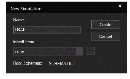
Creating a New Simulation Profile
To view the behavior of this circuit over time, transient analysis will be used. To perform this analysis, you will specify this analysis type when creating the simulation profile.
To create a new simulation profile, do the following:
- Choose PSpice – New Simulation Profile, or click the New Simulation Profile icon on the PSpice toolbar.
The New Simulation dialog box opens. - Specify the name of the new simulation profile as TRAN.
- In the Inherit From drop-down list, ensure that none is selected and click Create.
- In the product choices dialog box, select the OrCAD PCB Designer Professional w/PSpice option and click OK.
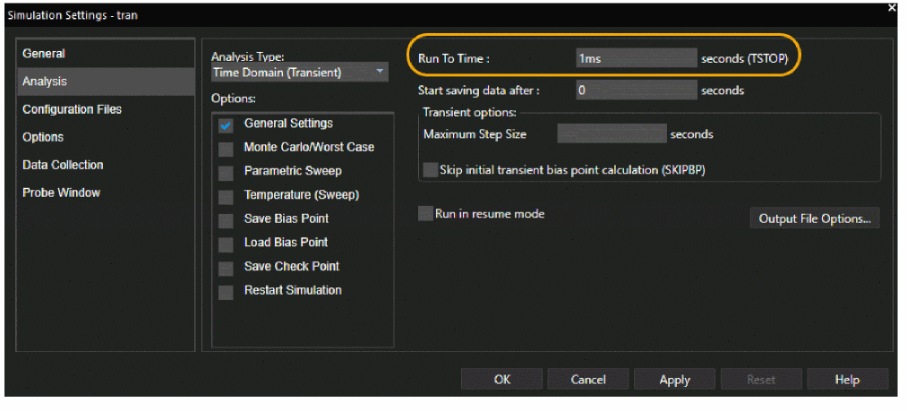
The Simulation Setting dialog box appears with the Analysis tab selected.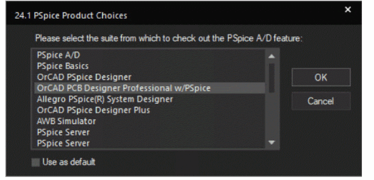
- In the Analysis Type drop-down list, Time Domain (Transient) is selected by default. Retain this default setting.
- To run a transient analysis, specify time as 1ms in the Run To Time text box.
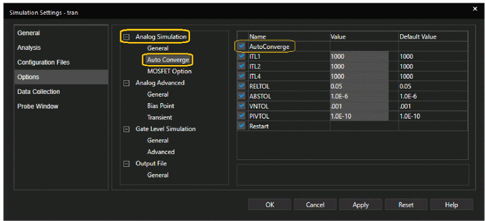
- To prevent any convergence issues, in the Options tab, select the Auto Converge check box under Analog Simulation.
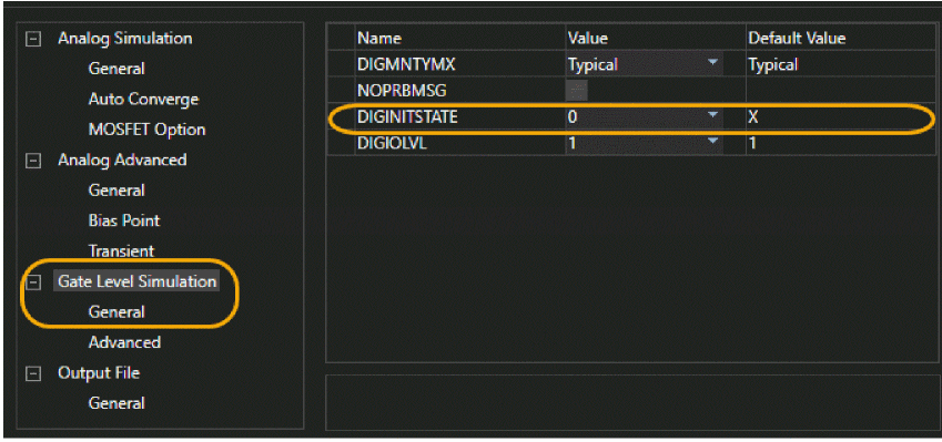
- To set the initial digital state of the simulation to 0, click Gate Level Simulation and set DIGINISTATE as 0.
- In the Configuration Files tab, select Stimulus from the Category list.
- Click the Browse button to navigate to the stimulus.stl file and click Open.
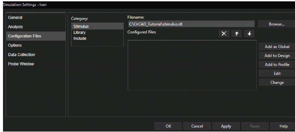
- Click the Add to Design button.
- Click OK to save your modifications.
When the simulation is run from the schematic, the simulator reads the SPICE models connectivity information (netlist) from the design files, and the analysis type and the stimulus details from the simulation profile.
Running the Simulation
- To simulate the design, choose PSpice – Run or click the Run PSpice icon.
The Schematic1-TRAN - PSpice window opens.
Viewing Output Waveforms
To visualize the circuit behavior and determine the validity of your circuit design, you can plot the output waveforms in the Probe window. By analyzing the output waveforms you can evaluate your circuit for performance.
For PSpice to display output waveforms in the Probe window, you need to place markers in your circuit design in Capture to indicate the points where you want to see simulation waveforms displayed in PSpice.
Markers can be placed:
- before simulation to limit results written to the waveform data file, and automatically display those traces in the active Probe window.
- during or after simulation, to automatically display traces in the active Probe window.
-
To add markers, choose PSpice – Markers or use the icons provided on the PSpice toolbar.
To view the markers in the simulation results, the schematic design must be open.
You will now add voltage markers to view the output waveforms in the Probe window. To do so:
- Select PSpice – Markers – Voltage Level, or click the Voltage/Level Marker icon on the PSpice toolbar.
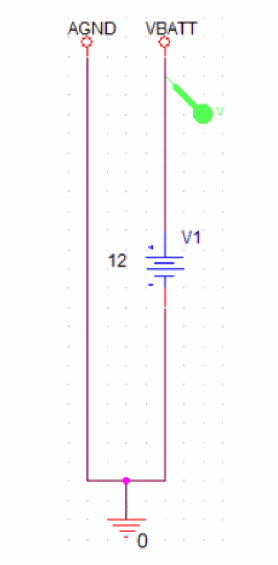
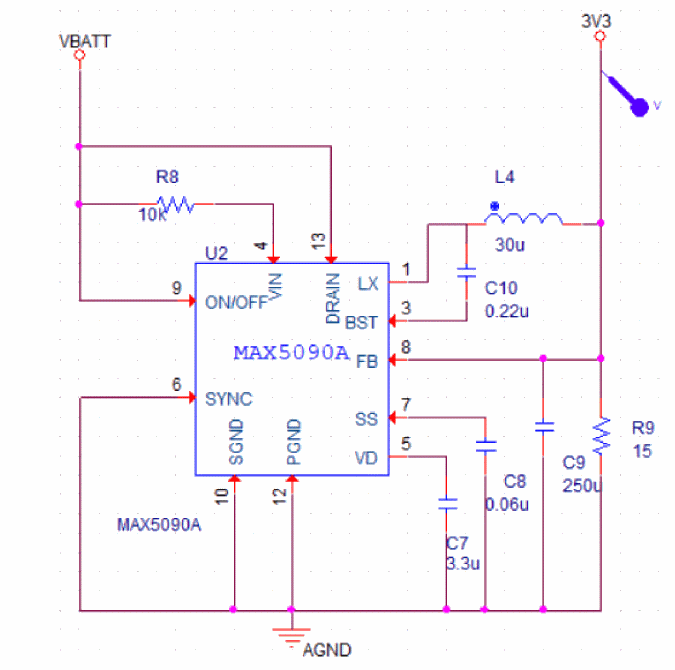
- Place the marker at the main power supply, that is at the 12 Volt VBATT power net.
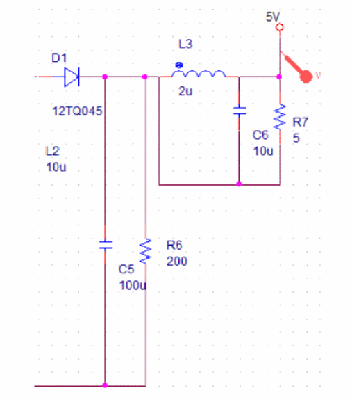
- Place the marker at the end of the first subdesign (12V to 5V converter) at the 5V power net, as shown in the following figure:
- Place another voltage marker at the end of the third subdesign (12V to 3.3V converter), at the 3V3 power net, as shown in the following figure:
If you add markers before simulating the design, the output waveforms are displayed automatically in the Probe window after the simulation is complete.
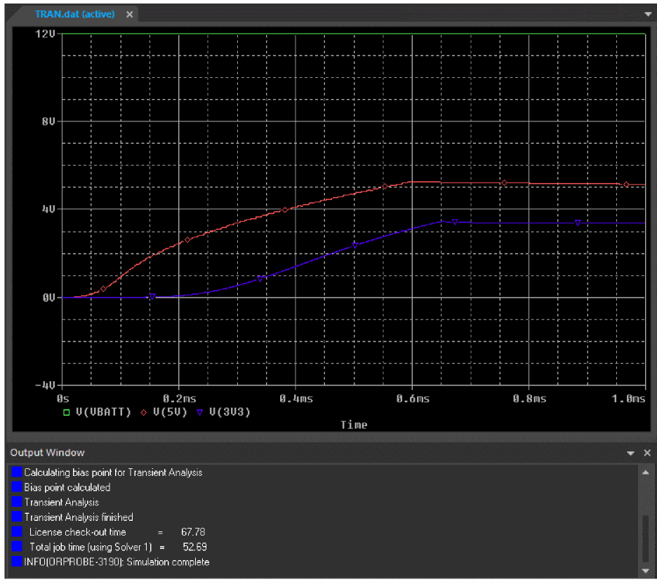
- Switch to the Probe window to view the output waveform.
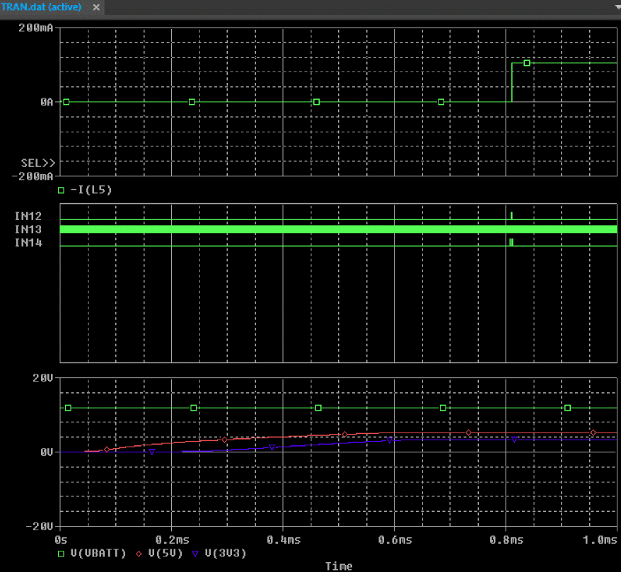
The output waveform appears as shown in the following figure:
Output Waveform - Probe window
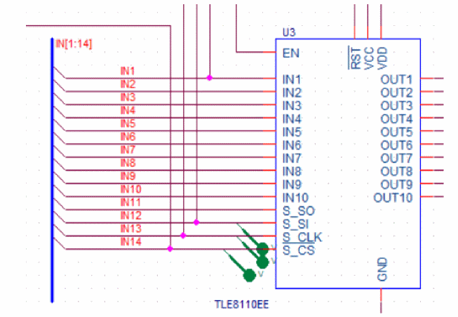
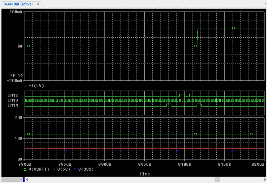
- To view the waveform of the digital stimulus sources at the input of the switching IC TLE8110EE, place voltage markers on the following nets:
- IN12 (connected to pin S_SI)
- IN13 (connected to pin S_CLK)
- IN14 (connected to pin S_CS)
- In PSpice, select Plot – Add Plot to Window.
- In Capture, place a current marker (using the Current Marker icon on the pin of the inductor as shown in the following figure:
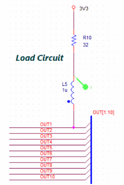
The changes in the waveform are displayed in the following figure:
The command to turn on the fan is sent to the S_SI pin. This command is read and executed at the low to high transition of the S_CS signal. The input signal through the S_SI pin is sent from the duration 808us to 811us, as shown in the following figure:
Summary
This section covered the steps to simulate the fan module design using PSpice. In this section, you were introduced to various tasks involved in the simulation process, such as creating a simulation profile, running simulation, placing markers, and analyzing simulation results.
View the next document: 03 - Preparing for PCB Layout Creation
If you have any questions or comments about the OrCAD X platform, click on the link below.
Contact Us