03 - Preparing for PCB Layout Creation
Now that you have verified the performance of your logical circuit through simulations, you can start designing the physical layout of the PCB board for this schematic design.
Before you create the PCB layout, you need to ensure that the design has no open or unconnected signals, footprint information is available for all components, and electrical constraints, if any, are specified.
Adding and Placing Connectors
To connect the fan module with a system, connector components are required to be placed in the schematic design.
To add and place connectors in this schematic design, do the following:
- Open your Capture CIS design.
- Select Place – Part, press P, or click the Place part icon (
 ).
).
The Place Part pane opens. - To add Connector.olb to the project, click the Add Library icon (
 ).
).
The Browse File dialog box opens. - Browse to <installation_directory>\tools\capture\library\Connector.olb.
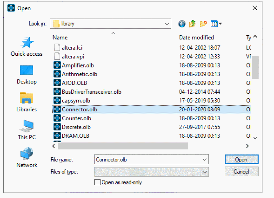
- Select Connector.olb and click Open.
The CONNECTOR library appears in the Libraries list box. - Search for CON2_M from the Part list box.
- Click the Place Part icon (
 ) or press Enter.
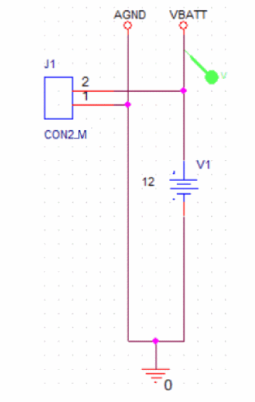
The part symbol is attached to the cursor. - Click the schematic page where you have placed the 12 volt DC source and place the connector J1 and press Esc.
- Right-click this connector and select Rotate and then connect it as shown in the figure below.
Connector at the main power supply
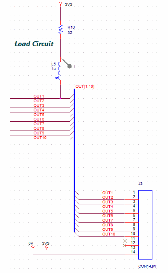
Similarly, add a 14-pin connector (CON14_M) to the input and output channels of the smart multi-channel switch IC.
To add the connectors in the smart multi-channel switch circuit, do the following:
- In the Place Part pane, search and select CON14_M from the Part list box.
- Click the Place Part icon (
 ) or press Enter.
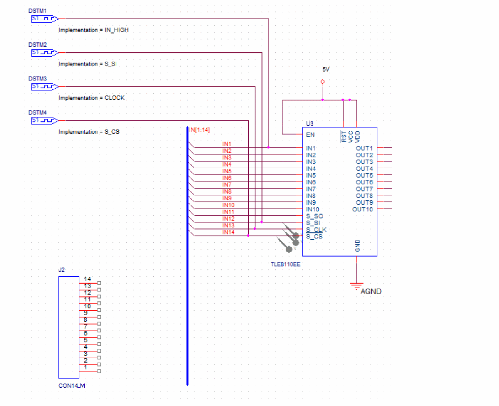
The part symbol is attached to the cursor. - Click the schematic page before the IC TLE8110EE and place the connector J2 as shown in the below figure.
- Right-click J2 and select Rotate.
- Extend the bus before the input pins of TLE8110EE as shown in the below figure.
Placing connector, J2
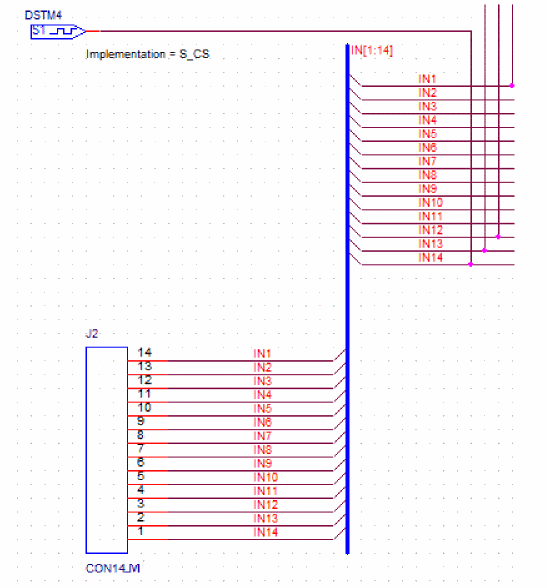
- Select all the pins of connector J2, right-click the selection, and choose Connect to Bus.
- Click the bus that you had extended in step 5.
The Enter Net Names dialog box appears. - Click OK.
Net names appear on each net from the connector pins to the bus.
Connecting J2 to bus at the input of TLE8110EE
- Similarly, place another connector, J3 and do the following:
- Connect its first 10 pins as shown in the figure below.
- Click the No Connect icon (
 ) or press X, and connect it to pins 11 and 12 of connector J3.
 - Connect 3V3 and 5V power ports to pins 13 and 14 of connector J3.
Connecting J3 to bus at the output of TLE8110EE
Updating Footprints
As the first step to preparing your design for layout creation, update the footprint associated with all the resistors in the design.
Updating Footprints Associated with Resistors
To assign footprints to all the resistors, do the following:
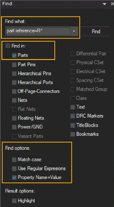
- Choose Edit – Find or press CTRL+F.
The Find pane appears. - Specify part reference=R* in the Find what field.
- Select the Parts check box under Find in.
- Select the Property Name=Value check box under Find options.
Specifying search criteria in Find pane
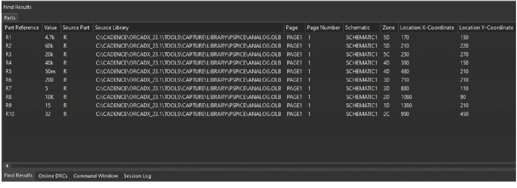
- Click the Find button.
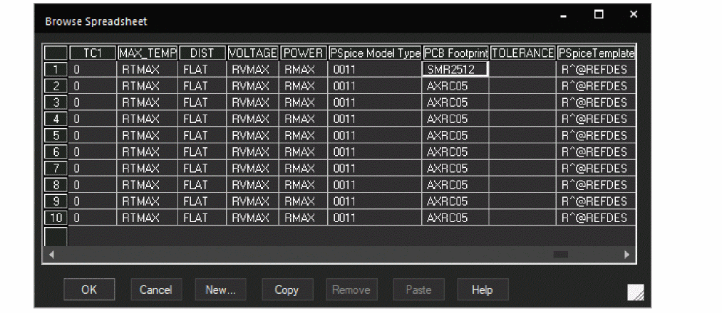
The Find Results window appears with a list of all the resistors in the design.
Viewing search results in Find Results window
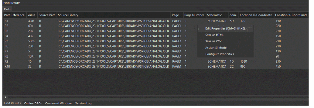
- To select all the rows in the Find Results window, click the first row, press SHIFT and then click the last row.
- To modify the properties of the selected results, right-click the selection and choose Edit Properties or press CTRL+SHIFT+E.
Editing properties of search results
The Browse Spreadsheet window opens.
- Change the value from AXRC05 to SMR2512 for PCB Footprint corresponding to each resistor.
Changing PCB Footprint values in Browse Spreadsheet window
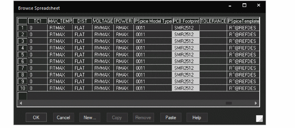
- Click OK.
An undo warning appears to confirm the changes.
- Select the Do not show this box again check box and then click Yes.
Updating Footprints Associated with Capacitors
Similarly, update footprints associated with all the capacitors with the following changes and save the design:
-
- Specify part reference=C* in the Find what field.
- Change the value from cap196 to SMC0603 for PCB Footprint corresponding to each capacitor.
Updating Footprints Associated with Inductors
Update footprints associated with all the inductors in the design with the following changes and save the design:
-
- Specify part reference=L* in the Find what field.
- Change the value from DISC350x1to SML0805 for PCB Footprint corresponding to each inductor.
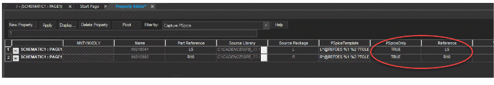
Configuring the PSpiceOnly Property
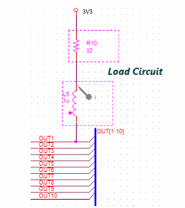
Some components are added only to represent the fan loads and are not required for the physical layout. To ignore them in the board design, you need to specify the PSpiceOnly property.
To assign the PSpiceOnly property to the inductor and the resistor of the load circuit, do the following:
- Select the inductor and resistor in the load circuit.
Selecting components of load circuit
- Right-click and choose Edit Properties.
- Click the Parts tab in the Property Editor window.
- From the Filter by drop-down list, select Capture PSpice.
- Right-click the cell for the PSpiceOnly property and choose Edit.
- Specify TRUE as the value in the PSpice Only cell and click OK.
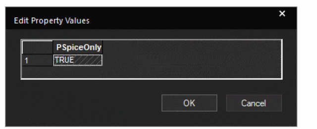
Parts tab in Property Editor Window
- Save the design.
Adding Constraints
You will now specify the minimum value of the total etch length of each net in Constraint Manager launched from Capture.
To add this electrical constraint in the schematic design, do the following:
- Choose PCB – Constraint Manager or click the Constraint Manager icon (
 ) on the PCB toolbar.
An information window appears to explain the Capture-Constraint Manager flow.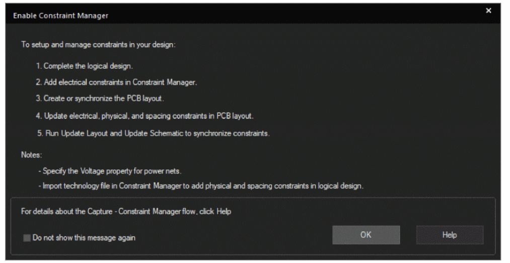
- Click OK.
The Migrate Constraints dialog box appears. - Select Migrate constraints from schematic design.
- Specify the unit to be used for physical and spacing constraints in the Constraint Manger window.
PCB Editor uses Mils as the default unit. For this tutorial, select Mils from the Units drop-down list.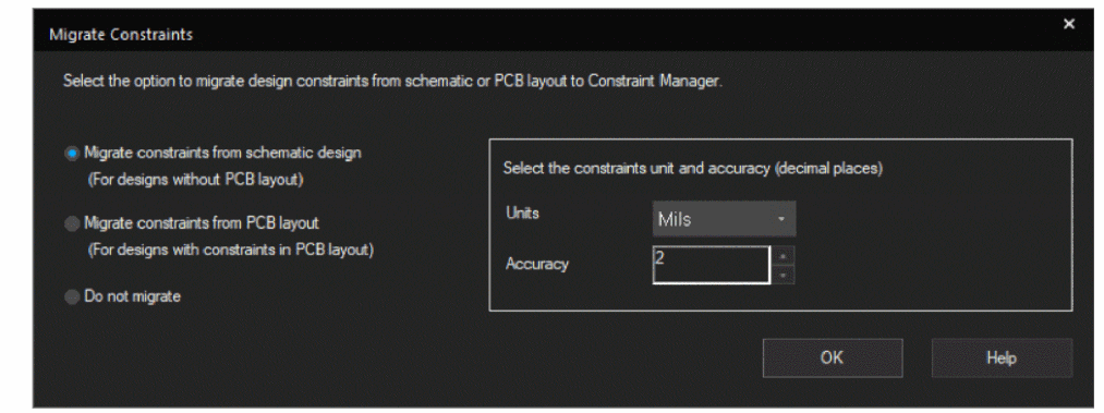
- Click OK.
The Assign Voltage to Power Nets window opens. This has predefined voltage values for all the power nets. - Modify these voltage values as follows:
- VBATT = 12V
- VCC=5V
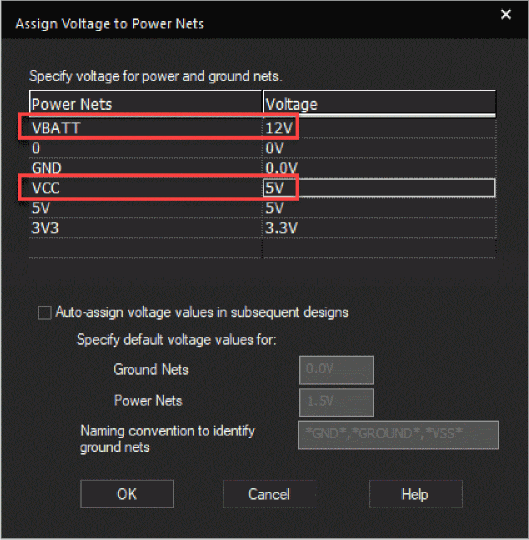
You can also open this dialog box from SI Analysis – Identify DC Nets.
- Click OK.
The Constraint Manager window opens.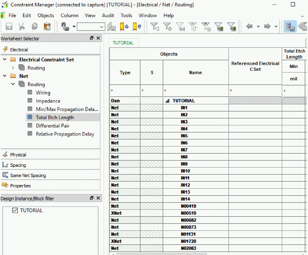
- Specify the minimum total etch length for the IN1 net as 100 mils as shown in the following figure:
Specifying minimum total etch length value in schematic design
- To specify the same value for Total Etch Length in all the nets, select the next row up till the last net in this window.
- Release the mouse and specify 100 in the last row.
All the nets and Xnets in the design are assigned the same value.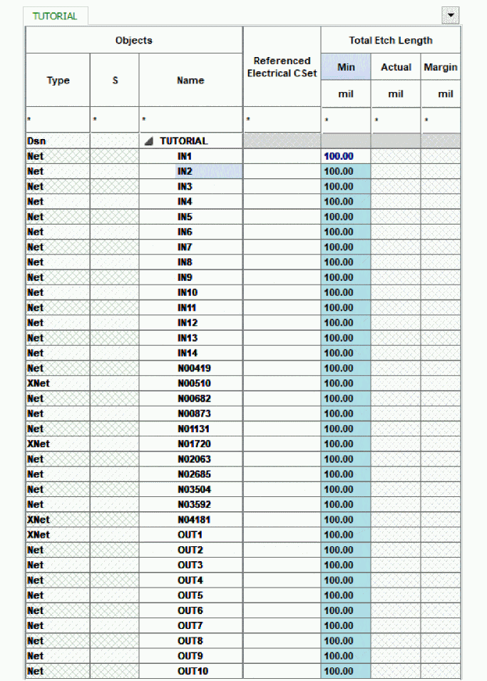
- Save the design.
Summary
This section covered the steps for preparing the schematic design for designing the physical layout of the PCB board. In the process, you were introduced to tasks, such as placing connectors, adding footprint information, and adding electrical constraints using Constraint Manager.
View the next document: 04 - Creating a Board Design
If you have any questions or comments about the OrCAD X platform, click on the link below.
Contact Us