01 - Creating a Schematic Design
In this section, you will create a schematic design for a fan-control module with three subdesigns as illustrated in the following figure:
Schematic design for the complete fan-control module
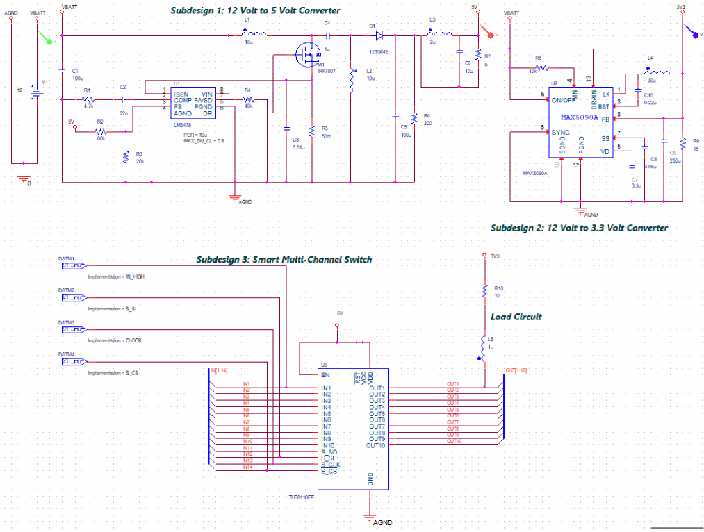
The following table provides a brief description of the function of each subdesign:
Subdesigns in the fan module circuit
| Subdesign | Function |
|---|---|
|
Subdesign 1 |
A step-down DC-DC converter. It uses IC LM3478, a low-side n-channel MOSFET controller for switching regulators, which converts 12 volt to 5 volt. The output of 5 volts is the internal power supply for this circuit. It provides supply voltage to IC TLE8110EE (in subdesign 3). |
|
Subdesign 2 |
A step-down DC-DC converter that uses the IC MAX5090A to convert 12 volt to 3.3 volt. |
|
Subdesign 3 |
A smart multi-channel switch, TLE8110EE powered by a 5 volt supply. This switching of IC, TLE8110EE can control multiple load types (fan load in this tutorial). It has 10 input channels and a serial peripheral interface (SPI). It has 10 output pins, which can control up to 10 fans. |
Creating a New Project
A project file (.OPJ) is a container for the design file (.DSN). In addition, a project file also includes simulation profile and layout information.
- To create a new project, click the Windows Start button (bottom left of your screen) and expand Cadence PCB 2024 folder.
- Double-click the Capture CIS 24.1 icon.
The 24.1 Capture CIS Product Choices dialog box opens.
-
Select OrCAD X Professional and click OK.
The OrCAD X Capture window opens. When you open Capture with an OrCAD X license, you are prompted to provide your login credentials to access OrCAD X-enabled features.This step is not mandatory for the purpose of this tutorial. You can skip this step by closing the login window and moving to the next step. - Choose File – New – Project.
- In the New Project dialog box, specify the project name as tutorial.
At the time of creating a new project, you can decide if you want to store the project in the OrCAD X Cloud workspace. If you select the Use Workspace option in the New Project dialog box, the Cloud workspace location is pre-seeded and cannot be changed later:
%HOME%\cdssetup\workspace\ - For the purpose of this tutorial, deselect the Use Workspace option.
- Specify the location as: C:\OrCADX_Tutorial.
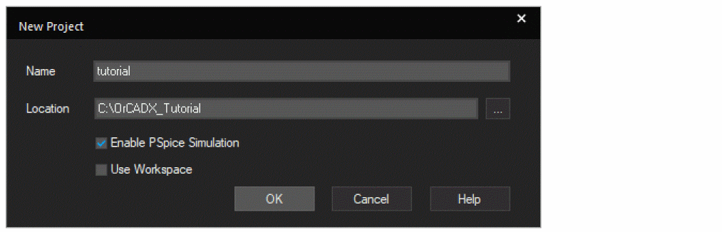 The Enable PSpice Simulation option is selected by default.
 - Click OK.
The Create PSpice Project dialog box opens. - Select Create a blank project.
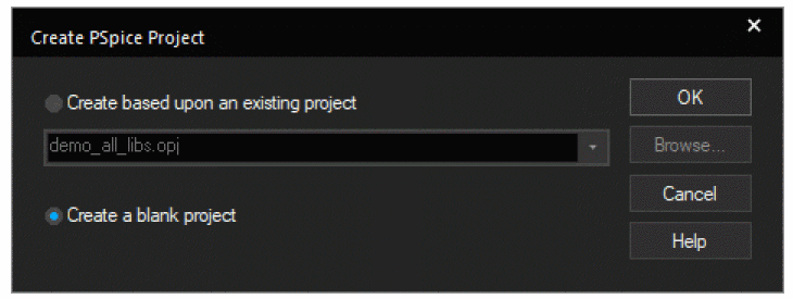
When you create a blank project, the project can be simulated in PSpice, but libraries are not configured by default. When you base your project on an existing project, the new project has the same configured libraries. - Click OK.
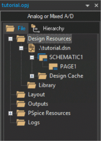
The tutorial project is created. In the project manager window, a design file, tutorial.dsn, is created. Under the design file, a schematic folder with the name SCHEMATIC1 is created. This folder contains a schematic page named PAGE1.
Project Manager Window
- Choose Options – Schematic Page Properties, and select the page size as B.
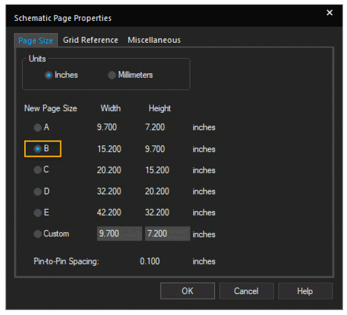
- Click OK.
Creating Design in Capture
You will now create the three subdesigns of the fan module.
| Subdesign No. | Instructions for subdesign creation are in the section... |
|---|---|
|
1 |
|
|
2 |
|
|
3 |
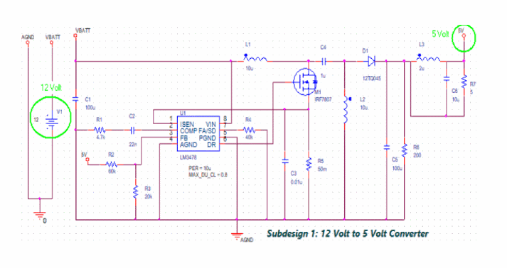
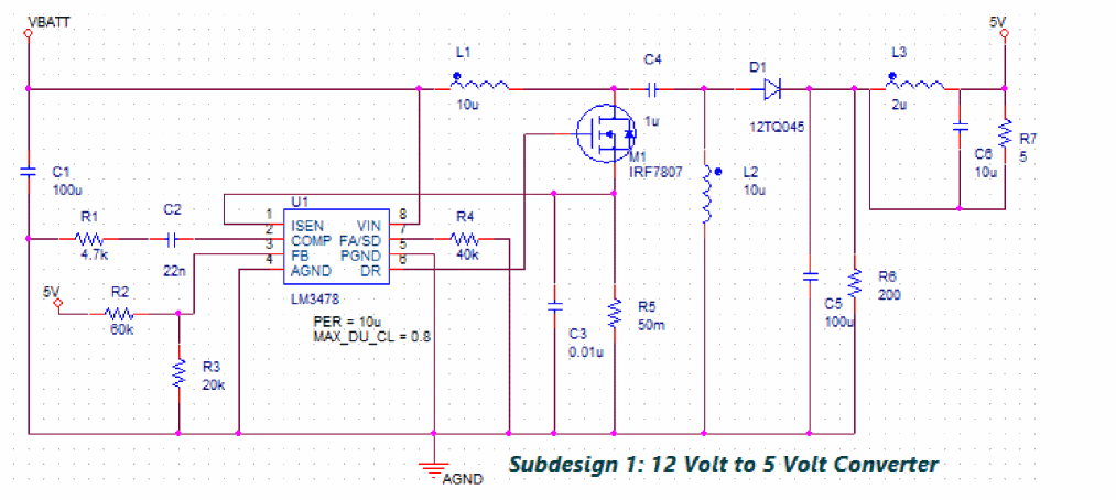
Subdesign 1: 12 Volt to 5 Volt Converter
Subdesign 1 consists of two parts, a 12 volt main power supply and a 12 volt to 5 volt converter as illustrated in the following image:
Subdesign 1: Main power supply and 12V to 5V converter
Part 1: Creating Subdesign 1A
To create the subdesign for the main power supply, you must place the components listed in the following table:
| Component | Source |
|---|---|
|
DC voltage source (V1) |
Place – PSpice Part – Modeling Application |
|
Ground symbols |
Place – PSpice Part – PSpice Ground |
|
Power ports |
Place – Power |
Placing Components for Subdesign 1A
- To instantiate an ideal DC voltage source on the schematic page(SCHEMATIC1:PAGE1), choose Place – PSpice Part – Modeling Application. Alternatively, click the Modeling Application icon (
 ) on the PSpice toolbar.
The Modeling Application pane opens. - Select Sources – Independent Sources.
- Click DC.
- Select Voltage and Ideal DC.
- Specify the value of DC Voltage as 12.
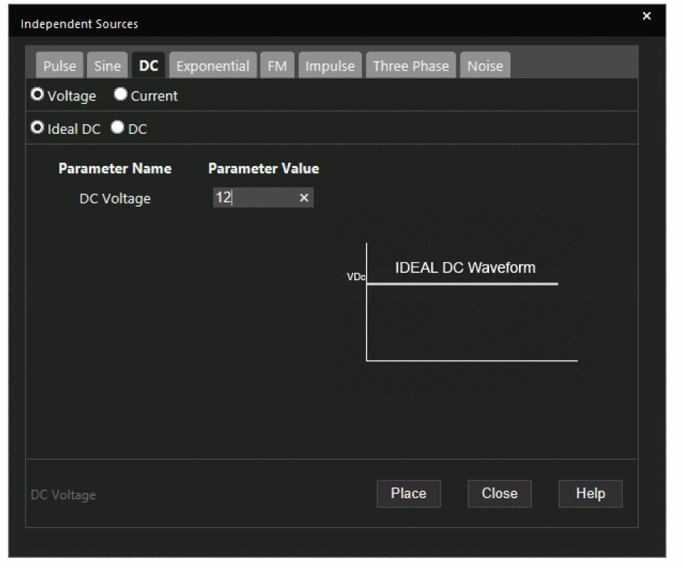
- Click Place.
The PSpice component is attached to the cursor. - Click to place the component on the schematic.
- To place a ground symbol, choose Place – PSpice Part – PSpice Ground.
- Click on the schematic page to place the part.
- Right-click and select End Mode or press Esc.
Next, you need to place a power port, VCC with its value set to VBATT, and another one with its value set to AGND from the CAPSYM library.
To place power components, do the following:
- Choose Place – Power. Alternatively, press f or click the Place power (F) icon (
 ) on the Draw Electrical toolbar.
 - Select CAPSYM from the Libraries list box.
- Select VCC from the Symbol list box.
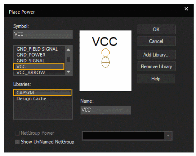
- Click OK.
- Click the schematic page to place this power port above the 12 volt DC source.
- Press Esc.
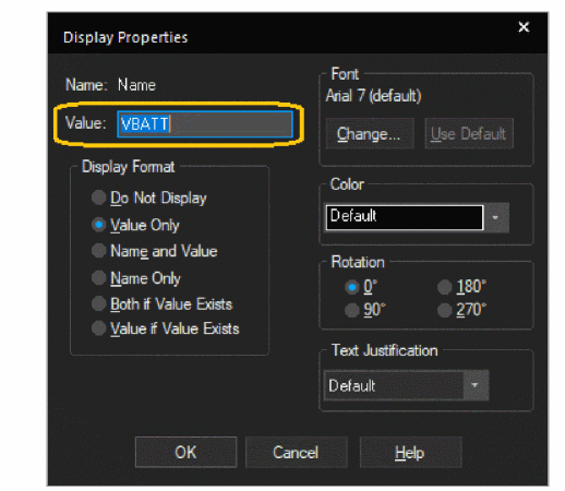
- Double-click VCC to open the Display Properties dialog box.
- Specify VBATT in the Value fields and click OK.
- Repeat steps 1 through 7 to add another power port, VCC, and set its value to AGND.
Connecting the Components
- Choose Place – Wire. Alternatively, press w or click the Place wire icon (
 ) on the Draw Electrical toolbar.
The cursor shape changes from pointer to cross-hair. - Draw the wire from the connection points of port AGND, PSpice ground, 12 volt DC voltage source, to the VBATT port as illustrated in the figure, Subdesigns in the fan module circuit.
Part 2: Creating Subdesign 1B
To create the subdesign for the main power supply, you must place the components listed in the following table:
| Component | Source |
|---|---|
|
DC-DC converter IC LM3478 |
Place – Component – Component Explorer |
|
MOSFET IRF7807 |
Place – Component – Component Explorer |
|
Power ports |
Place – Power |
|
Discrete components: Capacitor, Inductor, and Resistor |
Place – PSpice Part |
Subdesign 1B: 12V to 5V Converter
Placing Components for Subdesign 1B
- To place the DC-DC converter IC LM3478, choose Place – Component.
The Component Explorer interface opens. By default, the Cadence-supplied library, PSpice, is displayed. - Specify LM3478 in the Search here text box and press Enter or click the magnifying lens icon.
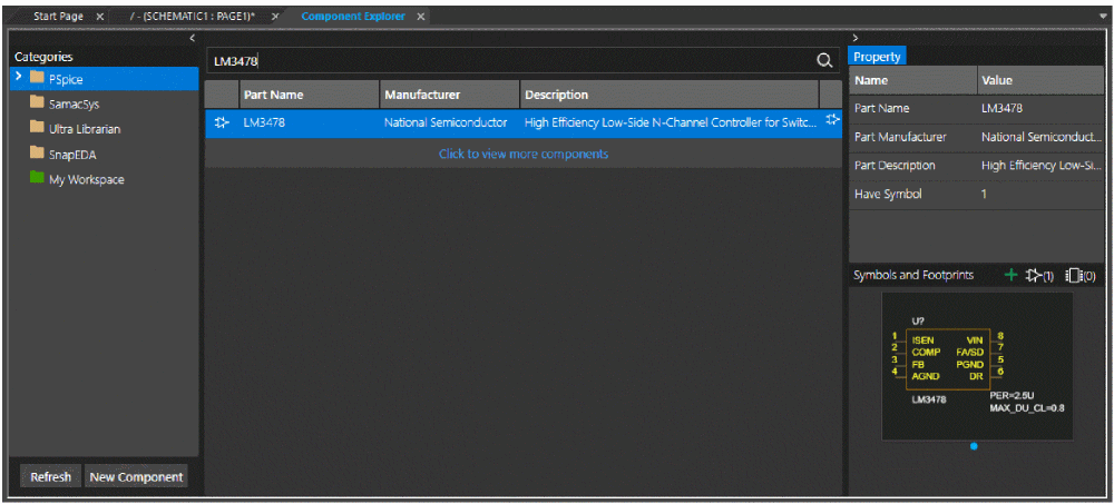
- Double-click LM3478 in the search results. Alternatively, right-click LM3478 in the search results and choose Place. You can also click the Place icon in the Symbols and Footprints bar in the right pane.
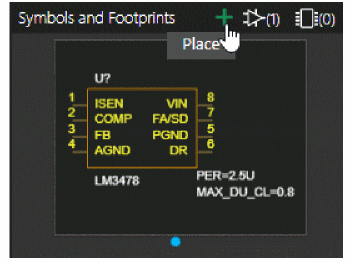
- Click the schematic page to place the converter IC.
- Right-click and select End Mode or press Esc.
- Double-click PER and set its value to 10u in the Display Properties dialog box.
This value sets the frequency of the IC. Changing the value to 10u (1/10u = 100KHz) sets the IC frequency to 100 KHz. - Follow steps 2-5 to place the MOSFET, IRF7807.
- Place the VBATT and the two 5V power ports shown in subdesign 1.
Placing Discrete Components
To place the commonly used discrete components, capacitor, inductor, and resistor, do the following:
- Choose Place – PSpice Part –
- Capacitor to place a capacitor.
- Inductor to place an inductor.
- Resistor to place a resistor.
- Click the schematic page to place each component and press Esc when done.
- To change the value of discrete components:
- Double-click their value to open Display Properties window.
- In the Value field, specify the required value of the discrete component.
- Click OK.
- Similarly, add other discrete components as specified in the following table:
PSpice Part Name PSpice Part Value C2
22n
R1
4.7k
R2
60k
R3
20k
R4
40k
L1
10u
C3
0.01u
C4
1u
R5
50m
L2
10u
C5
100u
R6
200
L3
2u
C6
10u
R7
5
- Search for 12TQ045 diode in the PSpice node in Component Explorer and place it on the schematic.
- Place the AGND port on the schematic.
Example - Placing the 100u Capacitor, C1
- Choose Place – PSpice Part – Capacitor.
- Click the schematic page to place the capacitor C1 below the VBATT port as shown in the figure, Circuit for smart multi-channel switch, TLE8110EE
- Right-click and choose End Mode or press Esc.
- Double-click the value, 1n.
The Display Properties dialog box opens. - In the Value field, specify the value of C1 as 100u.
- Click OK.
Connecting all the Components in Subdesign 1
- Draw a wire from pin 1 of LM3478 to the source of MOSFET M1, IRF7807.
- Draw a wire from pin 6 LM3478 to the gate of MOSFET M1, IRF7807.
- Draw a wire from 10u inductor, L1 to the drain of MOSFET M1, IRF7807.
- Similarly, add wires to the subdesign 1 until all the components are connected as shown in the figure, Subdesign 1B: 12V to 5V Converter.
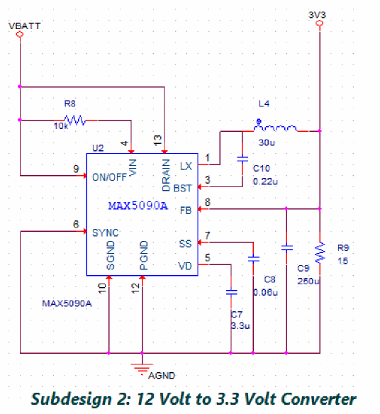
Subdesign 2: 12 Volt to 3.3 Volt Converter
The subdesign 2 of the fan module uses the IC, MAX5090A, which is a DC-DC converter that is down converting 12 volt to 3.3 volt. The output of 3.3 volt powers the fan.
Circuit for 12 Volt to 3.3 Volt converter
Creating Subdesign 2
To create subdesign 2, you must place the following components as listed in the following table:
| Component | Source |
|---|---|
|
DC-DC converter MAX5090A |
Place – Component – Component Explorer |
|
Ground symbols |
Place – PSpice Part – PSpice Ground |
|
Power ports |
Place – Power |
Component Placement for Subdesign 1A
- To place the DC-DC converter, MAX5090A.
- Choose Place – Component.
In the Component Explorer interface, the PSpice node is selected by default in the Categories pane. - Specify MAX5090A in the Search here text box and press Enter or click the magnifying lens icon.
- Double-click MAX5090A in the search results.
- Click the schematic page to place the component and press Esc.
- Choose Place – Component.
- Place the VBATT, AGND, and 3V3 power ports shown in figure, Circuit for 12 Volt to 3.3 Volt converter.
- Place the remaining discrete components in figure, Circuit for 12 Volt to 3.3 Volt converter) and specify their values from the following table:
PSpice Part Name PSpice Part Value L4
30u
C10
0.22u
R8
10k
C7
3.3u
C8
0.06u
C9
250u
R9
15
- Right-click C8 and choose Edit Properties.
- Set the value of IC as 0.
- Add wires to the subdesign 2 until all components are connected as shown in figure, Circuit for 12 Volt to 3.3 Volt converter.
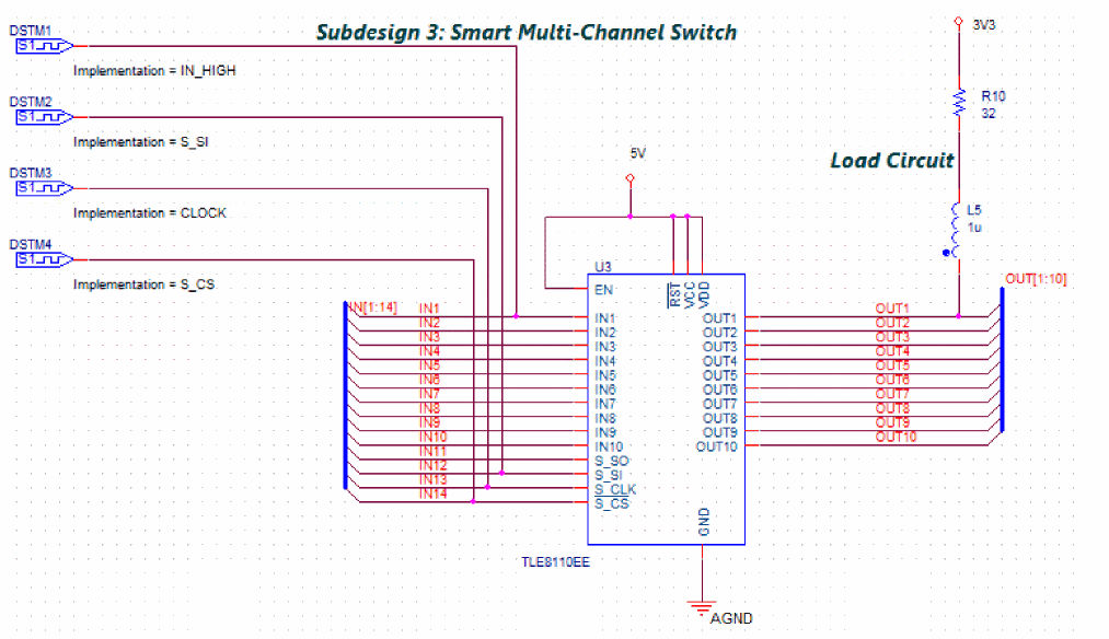
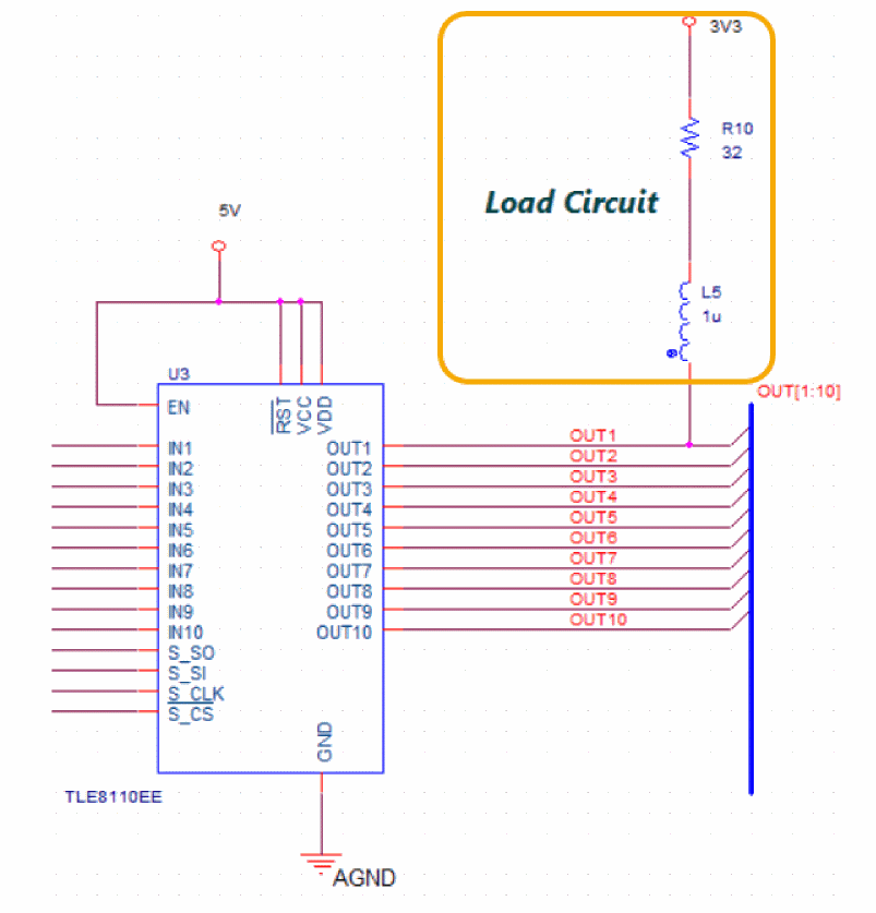
Subdesign 3: Smart Multi-Channel Switch Circuit
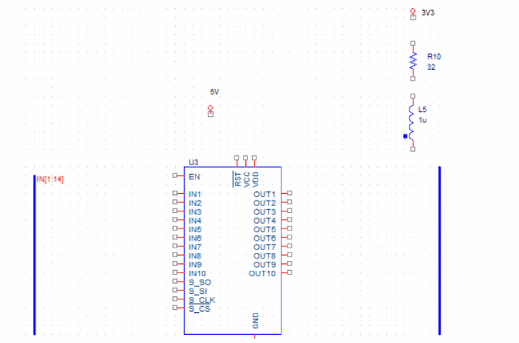
In subdesign 3, you will create the circuit for a smart multi-channel switch as shown in figure below.
In this subdesign an IC, TLE8110EE is placed to be interfaced with an off-board micro-controller. The input to the 10 channels of this IC are digital signals generated from a micro-controller. For this tutorial, these digital signals are modeled using digital stimulus sources.
Circuit for smart multi-channel switch, TLE8110EE
Creating Subdesign 3
To create the subdesign 3, you must place the following components as listed in the following table:
| Component | Source |
|---|---|
|
IC TLE8110EE |
Place – Component – Component Explorer |
|
Ground symbols |
Place – PSpice Part – PSpice Ground |
|
Power ports |
Place – Power |
|
Discrete components: Inductor and Resistor |
Place – PSpice Part |
|
Digital stimulus DIGSTIM1 |
Place – Component – Component Explorer |
Component Placement for Subdesign 3
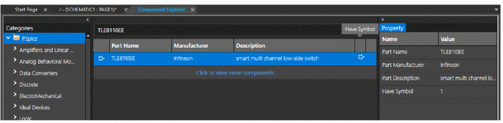
- Place the IC, TLE8110EE from the PSpice node of the Component Explorer interface.
- Place the AGND, 5V, and 3V3 power ports shown in figure, Circuit for smart multi-channel switch, TLE8110EE.
- Place the discrete components as shown in figure, Circuit for smart multi-channel switch, TLE8110EE and specify their values from the following table:
PSpice Part Name PSpice Part Value R10
This resistor forms the RL circuit for the fan type of load.
32
L5
This inductor forms the RL circuit for the fan type of load.
1u
- Place the digital stimulus sources from the PSpice node in the Component Explorer interface.
These are 1-bit digital stimulus sources.
To add these, search for DIGSTIM1 in the PSpice node of Component Explorer and select DigStim1 from the results.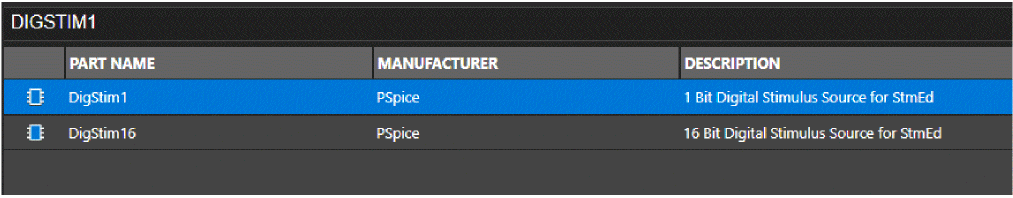
- Double-click the Implementation property of a digital stimulus source.
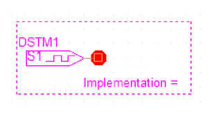
The Display Properties dialog box opens. -
In the Value field, specify the value of this Implementation property as shown in the following table:
Digital Stimulus Source Name Value of Implementation property DSTM1
IN_HIGH
DSTM2
S_SI
DSTM3
CLOCK
DSTM4
S_CS
The stimulus data from these sources is read from a .stl file.
Placing and Connecting Buses
- Select Place – Bus or press B. Alternatively, click the Place bus icon (
 ) on the Draw Electrical toolbar.
The cursor shape changes from pointer to cross-hair. - Draw the bus before the input pins and after the output pins of TLE8110EE as shown in figure, Placing Buses.
- Select Place – Net Alias or press N. Alternatively, click the Place net alias icon (
 ) on the Draw Electrical toolbar.
The Place Net Alias dialog box appears. - Specify the value in the Alias field as IN[1:14].
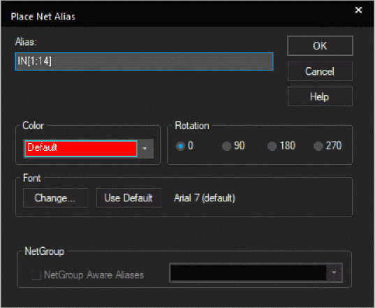
- Click OK.
- Move the cursor on the bus and place the net alias name as shown in the following figure:
Placing Buses
- Select all the input pins of TLE8110EE (except EN), right-click the selection, and choose Connect to Bus.
The cursor shape changes from pointer to cross-hair. - Click the bus placed before the input pins.
The Enter Net Names dialog box appears.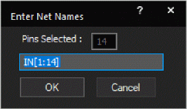
- Click OK.
Net names appear on each net from the input pins to the bus. - Repeat steps 3 to 10 to place the OUT[1:10] net alias on the bus placed next to the output pins of TLE8110EE, and to connect the output pins of TLE8110EE to this bus as shown in the following figure:
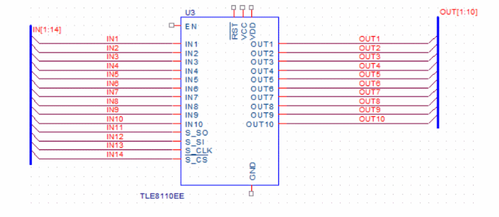
Connecting Components of Subdesign 3
- Draw a wires from the pins, RST,VCC, and VDD to the 5V power port.
- Draw a wire from the 5V power port to the input pin, EN of TLE8110EE.
- Draw a wire from the GND pin to the power port, AGND.
- Draw a wire from the output pin of:
- DSTM1 (with implementation=IN_HIGH) to net IN1.
- DSTM2 (with implementation=S_SI) to net IN12.
- DSTM3 (with implementation=S_CLK) to net IN13.
- DSTM4 (with implementation=S_CS) to net IN14.
- Connect the load circuit to the net, OUT1 as shown in the following figure:
Summary
This section covered the steps to create a schematic design using Capture CIS. In the process, you were introduced to some of the basic design creation tasks, such as creating a project, placing parts, editing property values, and connecting parts.
View the next document: 02 - Simulating a Design
If you have any questions or comments about the OrCAD X platform, click on the link below.
Contact Us