Home
Free Trial
Home
Free Trial
Read More
Content
Filter
10 results found
Featured
Section 16 – PCB Design: Vendor Management
Featured
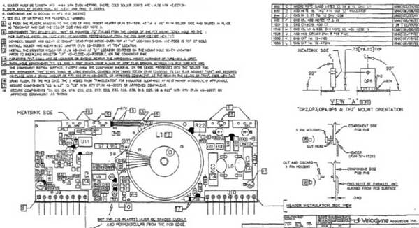
Section 15 – PCB Design: Creating a Document Package
Featured
Section 14 – PCB Design: Silkscreen Marking
Featured
Section 13 – PCB Design: Solder Mask
Featured
Section 12 – PCB Design: How to Design For Test
Featured
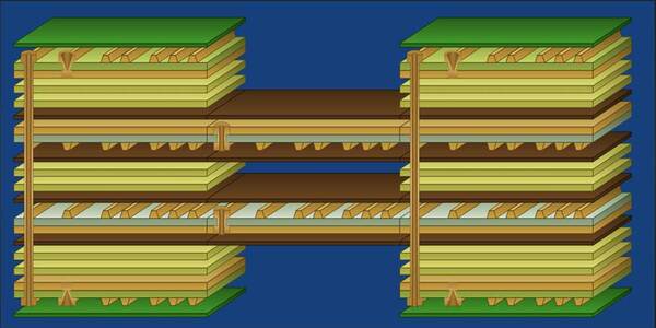
Section 11 – PCB Design: Multi-Board Systems
Featured
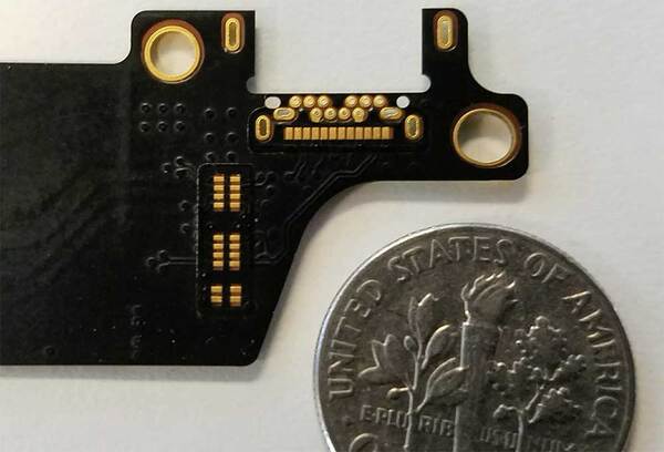
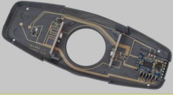
Section 10 – PCB Design: Flex Circuits
Featured
Section 9 – PCB Design: Analog Routing
Featured
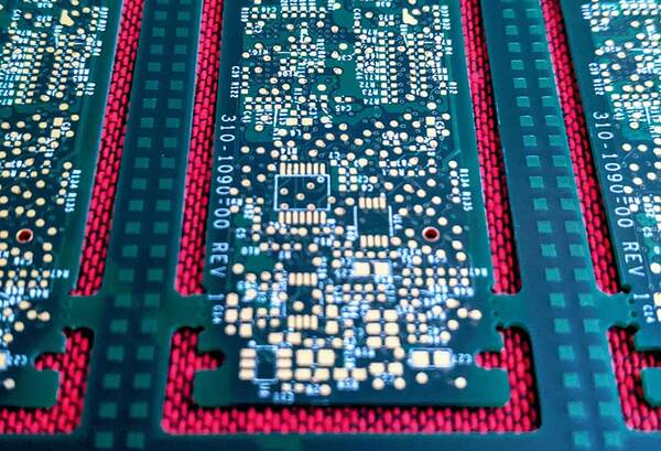
Section 8 – PCB Design: Memory Routing
Featured
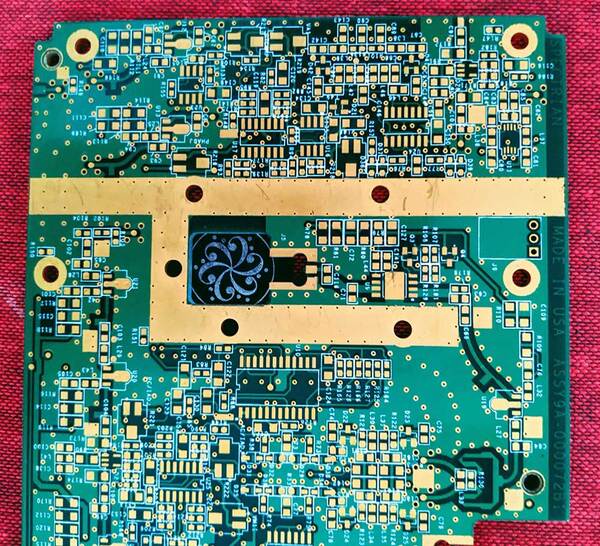
Section 7 – PCB Design: Understanding/Prioritizing Busses
Featured
Products
None
Content types
None
Blog
(10)
Solutions
None
PCB Layout
(6)