Maximize Performance With PCB Cross-Hatching
Key Takeaways
-
Cross-hatching significantly increases the flexibility of flex PCBs by reducing copper content.
-
Helps maintain optimal impedance in flex PCBs without altering dielectric thickness or signal line width.
-
Enables efficient manufacturing with reduced copper usage and improved resin adhesion.
Cross-hatch PCB connector
PCB cross-hatching is a technique where certain planes or large copper areas are designed to resemble a latticework, similar to a screen door with regular openings at set intervals. This method, though less useful in rigid PCBs today, has gained significant importance in flex and rigid-flex PCBs. In these applications, the cross-hatched ground pattern serves a dual purpose: it acts as both structural support and a grounding element, providing multiple benefits in such implementations.
Applications of PCB Cross-Hatching
|
Uses/Applications |
Details |
|
Controlled Impedance in Flex Regions |
|
|
Improved Structural Support |
|
|
Manufacturing Flexibility |
|
|
Copper Reduction |
|
|
Flexibility Enhancement |
|
PCB Cross-Hatching for Flex PCBs
The flexibility gained from cross-hatching planes in flex PCBs is directly proportional to the amount of copper removed. For example, if an application has four conductive layers with only one plane and the cross-hatch pattern removes just 30% of the copper on that plane, the increase in flexibility will be minimal. In contrast, if multiple planes are cross-hatched and 70% of the copper is removed, there will be a significant improvement in flexibility.
Cross-hatching also helps resolve adhesion issues in flex PCBs. This process creates small openings in the plane, allowing resins to bond effectively to the laminate. Unlike traditional methods that force resin to adhere to the copper, the cross-hatching technique ensures a strong, evenly distributed bond across the flex PCB, preventing delamination.
Cross-Hatching in Rigid PCBs
Cross-hatching is now rarely used in rigid PCBs. Historically, it was employed to address copper adhesion problems by creating small openings in the copper plane. These openings allowed resin to bond through the copper to the laminate, thereby preventing delamination. This practice is less common today, as adhesion technologies for rigid PCBs have advanced.
PCB Cross-Hatching Impedance Notes
The primary reason designers choose cross-hatched planes in flex PCBs is to manage impedance effectively. This design provides a return path for signals, resulting in optimal impedance without the need to increase dielectric thickness, select a lower dielectric constant, or reduce the signal line width. A cross-hatched flex PCB design helps maintain wide traces without compromising impedance.
Although flex PCBs have low dielectric constants, the laminate is very thin. Designers cannot achieve more than a 0.005-inch distance from the plane to the signals in a flex PCB design. While the line width can be reduced for mechanical reasons, this reduction negatively impacts the board's flexibility during bending.
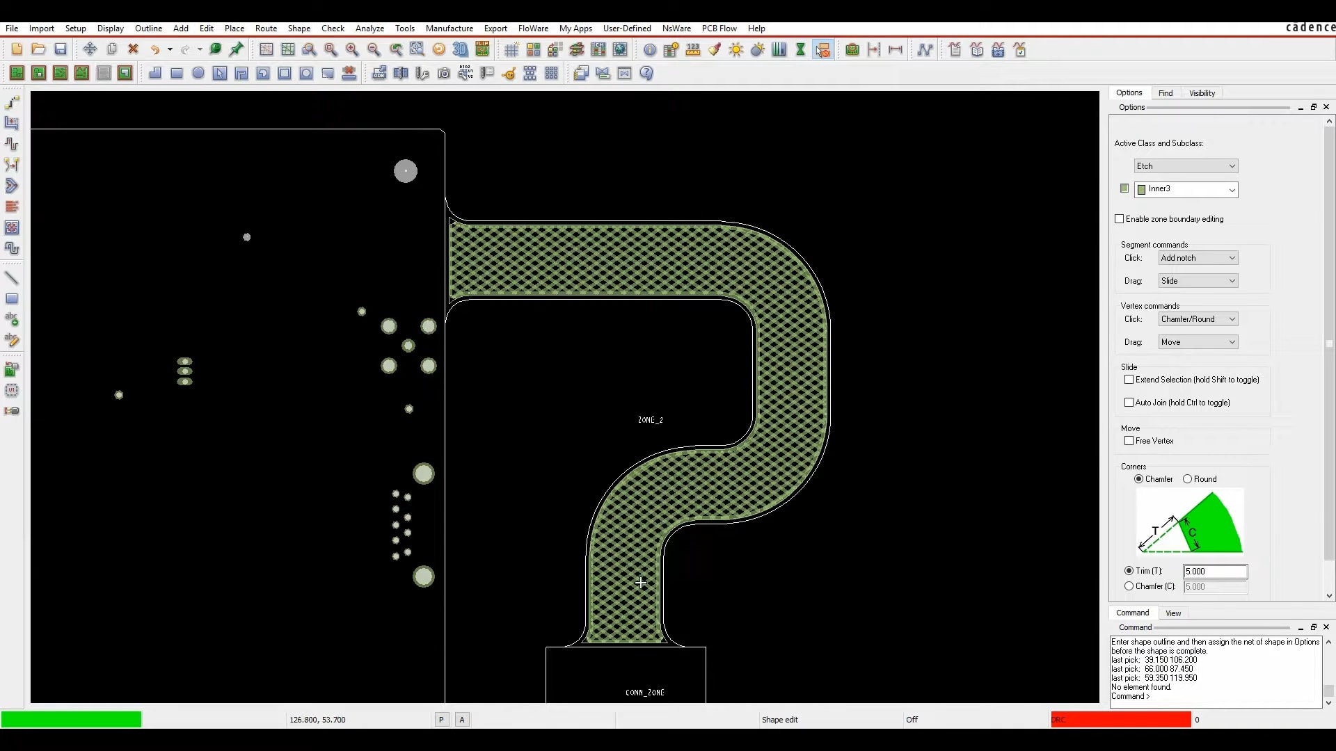
Choosing dynamic copper shapes in OrCAD X
Using OrCAD X For Intelligent Cross-Hatching
To accurately calculate a trace width that achieves the correct impedance, a modeling tool must be used to account for the copper missing in the cross-hatched plane. Since the impedance of a trace over a hatch ground region is higher than that over a solid ground region, the inductance of the trace must be reduced to maintain controlled impedance. This can be achieved by making the trace slightly wider, which will decrease the trace's inductance and increase the overall capacitance relative to the hatch ground, calculated through PCB software.
With OrCAD X, you can perform a variety of tasks related to cross-hatching for PCBs, particularly for flex and rigid-flex designs.
- Dynamic Cross-hatch Shapes: OrCAD X allows you to create dynamic cross-hatch shapes, which are particularly useful to prevent cracking when the board is bent. These shapes can also be used on main boards.
- Settings and Parameters: You can configure cross-hatch shapes by adjusting the pattern and its parameters. This includes setting the line width and spacing of the hatch pattern to fit specific design needs.
- Shape Creation: You can choose different shapes, such as rectangle, circle, or polygon, and apply dynamic cross-hatching to these shapes. The dynamic cross-hatch will automatically update when vias, pins, and other components are added to the design, unlike static cross-hatch, which requires manual updates.
- Layer and Net Assignment: When creating a cross-hatch shape, you can assign it to specific layers and nets within your PCB design. This ensures that the cross-hatch pattern is applied correctly to the intended areas.
PCB cross-hatching is a crucial technique for enhancing flexibility, structural integrity, and impedance control in flex and rigid-flex PCBs. Designers can leverage OrCAD X to optimize their cross-hatching patterns for superior performance. Explore the full capabilities of Cadence's PCB Design and Analysis Software and learn more about OrCAD X to revolutionize your PCB designs today.
Leading electronics providers rely on Cadence products to optimize power, space, and energy needs for a wide variety of market applications. To learn more about our innovative solutions, talk to our team of experts or subscribe to our YouTube channel.