PCB Layout Rules of Thumb for Consideration
Key Takeaways
-
Start with a complete plan - gather as much information upfront as possible
-
Map out your component placement for the best routing
-
Converting rules of thumb into design rules and constraints
Components placed on a printed circuit board, as viewed in a 3D PCB design system
Just because a “rule of thumb” is usually based on experience instead of precise facts doesn’t negate its value. For instance, when I told my kids that a good rule of thumb was to not back-talk to their mother, they discovered very quickly how accurate my advice was once they crossed that line. There are a lot of rules of thumb that we rely on daily, including those that apply to printed circuit board design.
While many aspects of PCB layout are governed by procedures, standards, and workflows, there is still much that belongs only to tribal knowledge. Unless this knowledge is collected, documented, and incorporated into a design database, it will only exist in the information that gets passed from one designer to the next. Let’s take a look at some of the more common PCB layout rules of thumb and see how they apply to the boards we are currently laying out.
The First PCB Layout Rule of Thumb: Start With a Plan
Something that you probably won’t ever find printed in a company procedure or a PCB design tutorial is the importance of having a plan before you start. Many layout designers have been known to plunge right into a new design, without first considering all the ramifications of what they are doing. This can lead to routing frustrations and eventual changes to the placement to complete the design correctly. To avoid problems like these, give some thought to what you are trying to accomplish before you start placing parts. Here are some ideas to consider:
-
Data: Gather as much information upfront as possible. The more you have to work with, the less chance there will be of having to re-do portions of the design.
-
Libraries: Make sure your PCB libraries are ready to go before you start placing components. A lot of design time gets wasted by having to re-layout circuitry to accommodate a modified or corrected part.
-
Schematic: Make sure that the schematic is relatively complete, updated, and ready to go. It is also very helpful if it is laid out logically, with components and nets clearly labeled and defined.
-
Parameters: Set up your design environment with preferred settings first so that you don’t have to go back and make adjustments to text or other details later on.
-
Workflow: Before you start, make sure that everyone on your team understands their responsibilities. Assign tasks to team members, organize the workflow, and arrange for additional help if needed.
With a plan in place, you can begin your layout without distractions that cost time and effort. Next, we’ll look at some rules of thumb for placing components on the board.
A PCB layout should start with a detailed plan to avoid problems completing the design
A Clean PCB Layout Begins With Placement
One rule of thumb to keep in mind is the placement of components drives the routing of a board, and not the other way around. PCB designers typically know this rule instinctively, but it is still an important point to make. And while parts will always have to be adjusted to help the routing, it is still essential that designers understand how important a good part placement is to the overall success of the design. Here are some additional placement rules that will help with this.
Floor Planning
Circuit boards typically have different types of circuitry that can be designated as digital, analog, and power supply. These can be further broken down into sub-groups and may cause huge signal and power integrity problems if the groups are mixed together. The best thing you can do is to floor plan, or partition the groups of circuitry in the design before you start placing components on the board. This will help you avoid problems with crosstalk, EMI, noise, and other integrity issues that can ruin an otherwise good-looking design. One way to do this is to set your design up for cross-selection between the schematic and the layout, so you can select groups of parts on the schematic to be grouped in the layout.
Component Placement
With the floor plan of the board ready, you now have a good plan of attack for your layout to work with. Now it is time to execute that plan by placing the components on the board using some additional PCB layout rules of thumb:
-
Keep analog and digital areas of circuitry separate from each other. Even though you’ve done this in your floor plan, be careful when it comes to the actual placing of the parts. Placement is an iterative process with changes constantly being made, and you could easily slip a part out of its preferred position.
-
Maintain separation between noisy power supply components and the digital circuitry they are supplying.
-
Work with your mechanical team to place larger memory and processor components to help dissipate heat evenly throughout the board.
-
Place analog and RF components according to the signal paths designated in the schematic. A resistor that is inline between a source and a load should be placed between those pins as much as possible.
-
Analog and power supply circuitry should have their components placed for the most optimum routing. The traces used in this circuitry often need to be short, direct, and wider than other traces to help reduce their inductances, resistance, and noise.
-
PCB parts also need to be placed to best facilitate their assembly to the board. Design for manufacturability (DFM) rules are often treated as rules of thumb, but they are critical to the success of the design. These rules should be confirmed with the manufacturer before starting PCB layout to ensure that the board can be built as designed.
Placement Considerations for Routing
Earlier we stated that the placement drives the routing, but it's equally true that routing has an impact on how the parts should be placed. For this reason, components also need to be placed with the following routing considerations in mind. Here are some of those rules of thumb:
-
Give yourself enough room for routing large data memory buses. Remember to allow for escape routing as well.
-
Place parts so that sensitive digital signals do not get routed through analog circuitry or analog signals through digital circuitry.
-
Make sure that there is enough room for sensitive signals such as differential pairs, which will need extra spacing to other routing.
-
Do not let your component placement force you to route traces across voids or splits in the reference ground plane. This will ruin the signal return paths and create noise on the board.
The good news is that many of these placement and routing rules of thumb can be set up in your CAD system as official design rules and constraints. We’ll examine that next.
Setting up the PCB design rules and constraints for differential pairs
Converting PCB Layout Rules of Thumb Into Design Rules and Constraints
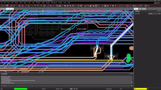
While simpler designs can sometimes be completed without a lot of automation, most PCB layouts today have too many requirements to keep track of them all manually. Fortunately, the rules of thumb that we discussed previously for component placement and routing can usually be set up as design rules and constraints in your CAD system. For example, the Allegro X PCB Editor from Cadence has a comprehensive design rule and constraint system built into it for this very purpose.
The Constraint Manager, shown above, provides an easy input tool for designers to legalize their rules of thumb. Starting with default values, the spreadsheet-style application allows you to set one value that will be propagated throughout or manually copy and paste entries as desired. The constraint manager, which is accessible in both the schematic and the layout, also allows the creation of classes that groups of nets or components can be added to. Trace widths and spaces, along with other constraints, can be added to individual nets or to the net classes. There are also high-speed design rules that can be set up, along with various fabrication and assembly rules to monitor part placement, silkscreen, solder mask, and paste masks. These rules are continuously reviewed by an online checking system while you design or they can be batch-checked as desired.
With the help of features like the Constraint Manager, PCB layout designers can rely on their systems instead of remembering multiple rules of thumb. The key, though, is to fully configure and put these features to work for you.
PCB design tools like Cadence Allegro X can easily cross-probe between the schematic and layout
Leverage the Power of Your Design Tools
We’ve already seen how tools like a Constraint Manager can help the designer, but that help is available only if the constraint manager has been set up with the necessary rules and constraints. Thankfully, PCB design tools can help you with this as well, as most of these tools provide a mechanism for importing and exporting their design rules. There are also many other features in the tools that can be automated, such as the setup of the different design parameters used for layout.
In the picture above, you can see how Allegro X will work with its schematic to cross-select components. A part has been selected in the schematic on the left, which has then automatically highlighted in red its layout counterpart on the right. By setting up your system to do this, you can quickly find and select the parts you need in the schematic and they will automatically cross-select in the layout.
These, and many other parameters, can be set up to help you incorporate your PCB layout rules of thumb into your PCB CAD environment, helping you to avoid costly mistakes and errors.
To find out more about circuit board design, take a look at our E-book on PCB layout.
If you’re looking to learn more about how Cadence has the solution for you, talk to us and our team of experts.