Where Can You Find Crosstalk in Your Designs?
What You Can Takeaway
-
Crosstalk arises due to parasitic coupling between conductors that carry electrical signals in a PCB.
-
The strength of crosstalk between different traces needs to be quantified and compared to design rules governing signal overshoot and undershoot to prevent signal degradation.
-
You can use a post-layout simulation tool to identify crosstalk, and your routing tools can be used to separate aggressor and victim traces in your PCB layout.

Easily analyze your design to check for crosstalk issues on critical nets.
Telecommunication equipment, RF boards for networking, boards for high speed processors, and many other systems have strict requirements on crosstalk intensity. The maximum crosstalk intensity is not always specified in a signaling standard, and it is not always obvious where crosstalk will be most intense in your design. As much as you might try to properly floor-plan your design, you may find that your layout and routing creates strong crosstalk from an aggressor trace.
So where can you find crosstalk in your design, and what is the easiest way to identify offending traces in your PCB? You could use a full-wave field solver, but there are easier analysis features you can use in your PCB design software to identify and suppress crosstalk. The best post-layout simulation tools for PCB design and layout will use a field solver with a reduced numerical algorithm to calculate crosstalk between nearby traces, giving you a quick way to spot crosstalk in your design.
The post-layout simulation features in Allegro are ideal for simulating signal behavior in your board, either before or after you finish your PCB layout. These features can be accessed within Allegro and take data directly from your layout; you won’t have to reconstruct your board in a separate simulation program. Here’s how you can access and use these features to analyze signal behavior and crosstalk within your design.

Where to Find Crosstalk in Your Design
Very simply, crosstalk can occur between any two conductors that carry signals in your PCB. This includes digital and analog nets. When crosstalk occurs, a signal on one conductor (the aggressor net) will couple a portion of itself as a new signal on a nearby conductor (the victim net). Digital and analog signals can induce crosstalk in different ways.
Crosstalk couples between signal nets in two ways, depending on the dominant type of parasitics that exist between two or more traces:
-
Capacitive crosstalk. This type of crosstalk occurs due to broadside parasitic and ground-coupled capacitance between two conductors. The magnitude of capacitive crosstalk is proportional to the parasitic capacitance between the two conductors. For analog signals, the strength of capacitively coupled signals increases with frequency, so this type of crosstalk can dominate in high frequency nets or when digital signals have very fast edge rates. Digital signals can induce capacitive crosstalk with transient ringing during and after switching.
-
Inductive crosstalk. This type of crosstalk occurs due to parasitic inductance between two loops of conductors. The magnitude of an inductive crosstalk signal from an analog aggressor signal is proportional to the rate at which the current in the aggressor trace changes (i.e., proportional to signal frequency). Digital signals can induce inductive crosstalk during switching, during which time the magnetic field emitted from the signal induces a changing flux in the victim net.
Inductive and capacitive crosstalk depend on the mutual inductance and mutual capacitance between two traces, respectively. These terms are determined entirely by the magnetic and electrostatic interactions between different conductors, as well as how these conductors are arranged in space. What this means is that you need to analyze crosstalk in a post-layout simulation; you can’t do anything to spot crosstalk from your schematics.
Spotting both types of crosstalk requires some unique analysis steps. You can try to quantify the different types of crosstalk with an analytical equation of the crosstalk coefficient, which will tell you the fraction of the aggressor signal level induced on the victim net. However, these will inevitably be approximations as the geometry in a real PCB layout can get very complicated, making the mutual inductance and mutual capacitance difficult to determine exactly. The better option is to use a post-layout simulation tool directly from your PCB design program.
Tools for Identifying Crosstalk in a PCB Layout
Once you’ve completed your PCB layout, you can take steps to try and identify nets that may experience large amounts of crosstalk. Because of the complicated geometry in any PCB, there are multiple parasitics on any given net, and you may see strong crosstalk even though you followed basic trace width and separation rules. In a dense board with hundreds of nets, you don’t need to simulate crosstalk between every trace. Instead, you only need to select critical nets as victim traces and look at nearby nets that may act as aggressor traces.
To do this in Allegro, you want to use two important simulation tools to analyze crosstalk:
-
Coupling analysis. The goal in this analysis is to determine the coupling coefficient between two traces and take steps to reduce the coupling coefficient if it is too large.
-
Crosstalk analysis. As its name suggests, this involves a direct simulation of a crosstalk signal from an aggressor to a victim. This is a time-domain simulation that will show you the exact waveforms introduced on the victim net due to crosstalk.
Coupling Analysis
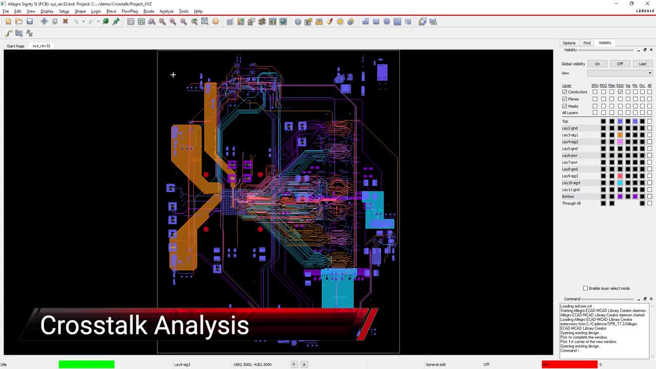
The coupling analysis tool can be accessed from the Signal Integrity program in Allegro. When this tool is run, the user selects nets to be analyzed. Once the results are calculated, they can be viewed in a table format and in a visual format within your layout. The coupling length and strength between a victim net and its aggressor net can be seen in your layout as a heat map, allowing you to pinpoint which nets need to be corrected.
In the image below, the net N22287555 has the strongest coupling with VDDS, which indicates noise in the digital power plane can easily couple into this net. The net USB0_ID has strong coupling to net N22155575. These two nets are on different layers, but they are not separated by a ground plane. This should illustrate the effects of placing ground planes between signals on different layers; it reduces the strength of potentially coupled signals. The specific region where high coupling is present can be identified visually using the heat map, which shows you which region of your routing may need to be adjusted to suppress crosstalk.
Coupling analysis results directly from a PCB layout. The heat map shows different regions with strong
Crosstalk Analysis
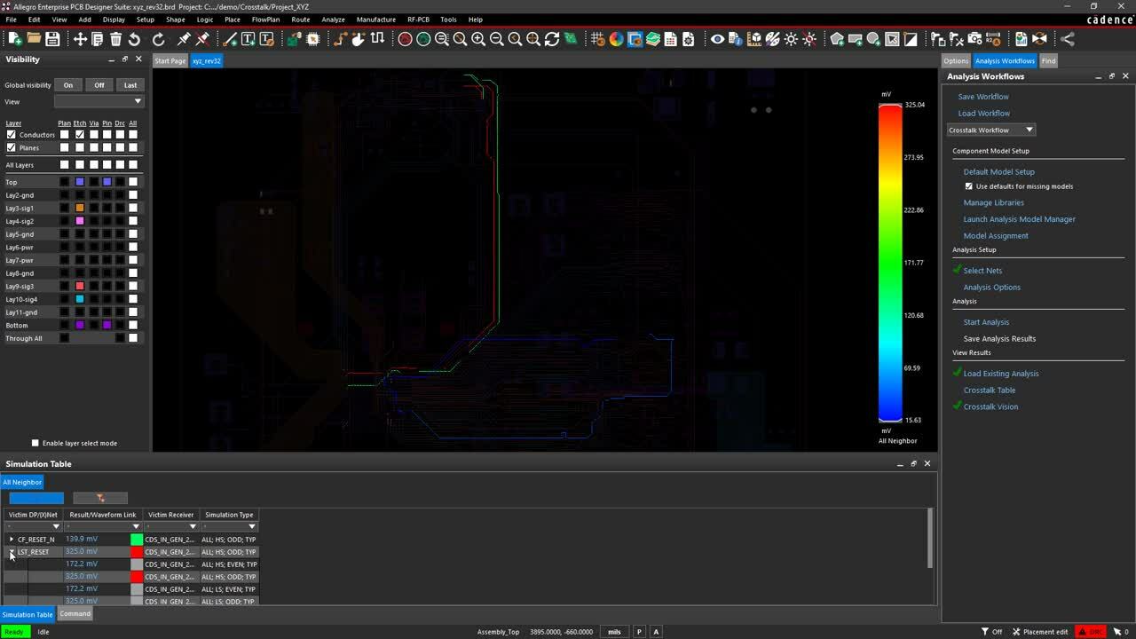
Coupling analysis allows you to identify which nets may exhibit strong coupling, while crosstalk analysis shows you the strength of any coupled signal. The same tools in Allegro that run coupling analysis also run crosstalk analysis. Simply run the tool from the Signal Integrity program and select the nets you want to analyze. The tool will return graphical and tabular results showing the coupled signal strength between the various nets you selected. Note that this analysis will show you the coupling region and the coupling coefficient, just as was done in coupling analysis.
Allegro analysis results directly from a PCB layout. The heat map shows exactly where crosstalk is introduced, and the table shows the induced signal strength in this region.
Solving Crosstalk Problems in Your PCB Layout
Once you’ve identified nets that are susceptible to crosstalk, you need to separate victim and aggressor traces or provide greater isolation between them. You can never totally eliminate crosstalk, but you can reduce it to the point where it does not cause unintended switching at the receiver (for digital signals) or excessive waveform distortion (for analog signals). This can be done in a number of ways:
-
Increase spacing between traces. Crosstalk is proportional to the strength of the electromagnetic field between two traces. Increasing the spacing between the victim and aggressor trace will decrease the field strength seen by the victim, which will then decrease the strength of a coupled crosstalk signal.
-
Route victim traces on a different layer. If you created your stackup to support high speed signals, you’ll most likely have interleaved signal layers between plane layers. The plane layers will provide natural isolation between different signal layers. You can route a victim trace or differential pair in a different signal layer if there is no room to move the signal path on its current layer.
-
Move traces closer to the ground plane. The ground plane distorts the electric and magnetic fields produced by the aggressor trace and increases isolation between them.
-
Place a guard trace or via fence between offending traces. Placing a grounded trace or via fence between two traces provides some shielding, just like using a ground plane. Whenever you place an isolation structure, it’s always best to quantify the effects of the structure using a 3D EM field solver.
Note that crosstalk is a reciprocal process; if two traces carry the same type of signal, the victim trace will induce the same crosstalk signal on the aggressor trace. This means that solving a crosstalk problem for one net will also suppress crosstalk on its aggressor.
Switching from a surface microstrip to stripline means the stripline will produce less crosstalk as it is surrounded by conductors, and it will be shielded from surface microstrips. In general, if you switch from microstrips to striplines with the same characteristic impedance and spacing, the striplines will experience less crosstalk than the microstrips.
Whether you route the victim signal on a different layer or increase spacing, you may need to check length matching in your traces. Routing through a via produces additional propagation delay, which can induce skew in parallel nets or differential pairs. Note that you can route one end of a differential pair through an internal layer if you like as long as you maintain differential impedance.
Once you’ve changed your routing or layer stack, check your layout again using the Crosstalk Analysis and Impedance Analysis workflows in Allegro. This will ensure you’ve maintained impedance control while reducing crosstalk to an acceptable level.
You can easily spot phase mismatches while routing differential pairs or parallel nets with Allegro’s routing tools.
If you’re looking to learn more about how Cadence has the solution for you, talk to us and our team of experts.