Buck Converter Simulation with PSpice
Key Takeaways
-
Buck converters efficiently step down DC voltage and are essential in countless electronic devices.
-
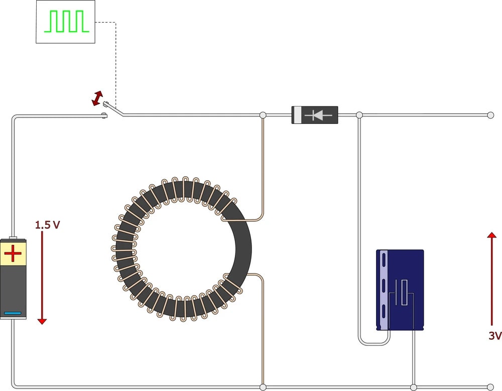
Buck-boost converters provide voltage step-up or step-down capability with output inversion. They require careful simulation to manage ripple and confirm correct polarity.
-
Synchronous buck converters offer higher efficiency through MOSFET-based rectification, but require careful attention to dead-time to avoid shoot-through.
A buck converter is a DC-DC converter that reduces voltage from a higher level to a lower level. Buck converters manage power delivery in applications, stepping down voltage in your laptop, phone, and essentially a zillion other devices. But before you commit to a design, you want to be sure it'll actually work as expected. Buck converter simulation is the key here, allowing you to virtually test and refine your circuit under various conditions. That’s where PSpice comes in, offering a comprehensive environment to model and analyze your converter's behavior before you ever build a physical prototype.
What is a Buck Converter?
The buck converter is a fundamental non-isolated DC-DC converter that achieves voltage step-down through controlled switching action and energy storage elements. Here’s the basic topology:
-
A DC voltage source (Vin)
-
A switch (i.e., a MOSFET)
-
A diode
-
An inductor (L)
-
A capacitor (C)
-
A load resistor (R)
Operating in continuous conduction mode (CCM), the converter alternates between two states: the switch (typically a MOSFET) is on, allowing the input voltage to forward bias the diode and energize the inductor, and the switch is off, forcing the inductor current to flow through the diode, replenishing the output capacitor and supplying the load. The duty cycle (D) of the switch dictates the theoretical output voltage, ideally Vout = D * Vin, neglecting losses.
From a buck converter simulation standpoint, several aspects should be analyzed:
-
Steady-State Output Voltage: Assessing the output voltage under varying input voltage and load conditions is crucial. Deviations from the ideal Vout = D * Vin indicates losses and non-ideal component behavior.
-
Switching Node Waveforms (Vds, Ids): Examination of the MOSFET's drain-source voltage (Vds) and current (Ids) waveforms reveals switching losses (turn-on, turn-off), ringing, and potential voltage overshoot, which can stress the device. Simulation enables optimization of gate drive circuitry and snubber networks to mitigate these effects.
-
Inductor Current Ripple (ΔIL): The inductor current ripple directly impacts output voltage ripple and EMI. Simulation allows for the calculation of ΔIL based on inductance (L), switching frequency (fsw), and duty cycle (D), guiding the selection of appropriate inductor values.
-
Transient Response: Evaluating the converter's response to step changes in load current reveals overshoot, undershoot, and settling time, allowing for optimization of the control loop to achieve fast and stable transient performance.
Buck Converter Types Compared
|
Converter Type |
Topology |
Differences when Analyzing Simulation |
|
Basic Buck Converter |
|
|
|
Buck-Boost Converter |
|
|
|
Synchronous Buck Converter |
|
|
Buck Converter Simulation
Let's start with a basic buck converter and walk through the process of how you would simulate an example buck converter from scratch using OrCAD X Capture and PSpice.
1. Project Setup & Placing Components
-
Create a New Project: In OrCAD X Capture, Go to File > New > Project.
-
Enable PSpice Simulation: In the New Project dialog, enable "PSpice Simulation."
-
Open Component Placement: Press P on your keyboard, or go to Place > Part.
-
Place Ground: Type "GND" in the search box and place a PSpice ground symbol on your schematic. You may need multiple grounds.
-
Place Components: Use the search option to find and place the following components from the PSpice libraries:
-
-
Resistor (R): For both the load and the gate resistor. Rotate with R.
-
Capacitor (C): For the output capacitor.
-
DC Voltage Source (VDC): For the input voltage.
-
Pulse Voltage Source (VPULSE): To drive the MOSFET.
-
MOSFET (i.e. IRF840): N-channel MOSFET.
-
Diode (i.e., MUR460): A fast recovery diode for the freewheeling diode.
-
-
Component Placement Example:
-
-
Place the components in a configuration, similar to the standard buck converter topology.
-
Place the VPULSE source, which will go through the gate resistor to the gate of the IRF840 MOSFET.
-
Place the MUR460 diode as the "flywheel diode". Ensure you select the correct one.
-
2. Set Component Values
The specific component values in a buck converter design depend on the application's requirements and performance goals. For this simulation, we'll use component values that target a moderate power level, a 20 kHz switching frequency, and a 50% duty cycle, but remember that these values can be adjusted to meet different needs.
-
Inductor Value: Set the inductor value (i.e., 500 µH).
-
Capacitor Value: Set the capacitor value (i.e., 50 µF).
-
Load Resistor Value: Set the load resistor (i.e., 10 Ω).
-
Gate Resistor Value: Set the gate resistor (i.e., Ω).
-
Input Voltage: Set the DC voltage source (VDC) (i.e. 100V).
-
Pulse Source Settings: Configure the pulse voltage source (VPULSE). Example parameters may be:
-
-
Turn-off Voltage (V1): -1 V
-
Turn-on Voltage (V2): 8 V
-
Time Delay: 0
-
Rise Time: 1 ns
-
Fall Time: 1 ns
-
Pulse Width: 25 µs
-
Period: 50 µs (This corresponds to a frequency of 20 kHz).
-
-
3. Wiring the Circuit
-
Enter Wiring Mode: Press W on your keyboard, or go to Place > Wire.
-
Connect Components: Wire the components together to form the buck converter circuit.
-
Net Aliases: Add net aliases (labels) to important nodes for easy measurement.
-
Place a net alias named "out" at the output node (after the capacitor).
-
Place a net alias named "in" at the input node (before the inductor).
Gate Voltage Consideration: The voltage difference between the gate and source of the MOSFET should be at least 8V to ensure proper switching.
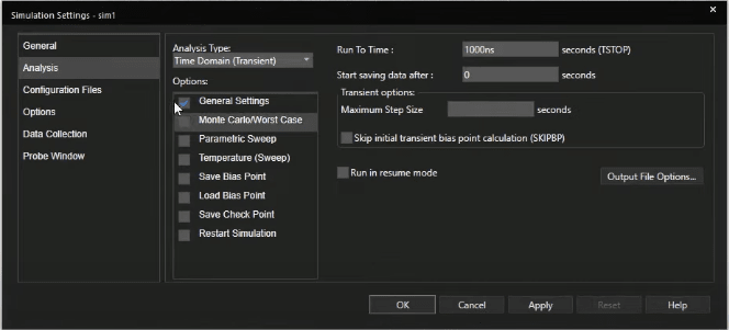
4. Simulation Setup
-
Save the Design: Save your schematic design.
-
Create a New Simulation Profile: Go to PSpice > New Simulation Profile.
-
Simulation Settings: In the Simulation Settings dialog, you can edit the options:
-
Analysis Type: Choose "Transient."
-
Run Time: Set the run time to 6ms (milliseconds).
-
Maximum Step Size: Leave blank for automatic selection, or set it to a small value (e.g., 1us) for more accuracy.
Apply and OK: Click "Apply" and then "OK" to save the simulation profile.
5. Run Simulation and Analyze Results
-
Run Simulation: Go to PSpice > Run.
-
Add Voltage Markers: Add voltage markers to the schematic to measure the voltages at different points in the circuit.
-
Voltage Differential: Use voltage differential markers to observe the voltage difference between two points. This can be useful for observing the gate-source voltage of the MOSFET.
-
View Waveforms: The simulation results will open in a separate window.
-
Adjust Trace Width: If the traces are too thin, right-click on a trace, choose "Trace Property," and change the width for better visibility.
-
Zoom and Analyze: Use the zoom tools to examine specific areas of the waveforms.
-
Examine the Following:
-
Output Voltage: Check if the output voltage is close to the expected value (e.g., for a 50% duty cycle, it should be around half the input voltage).
-
Ripple Voltage: Observe the ripple voltage on the output.
-
Rise Time and Settling Time: Analyze the rise time and settling time of the waveform.
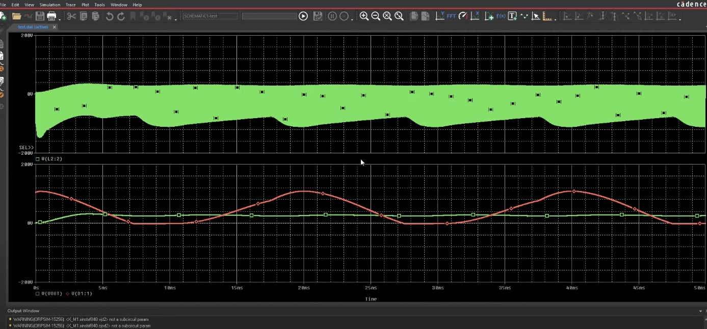
PSpice showing the expected output voltage with a small ripple factor
Buck-Boost and Synchronous Buck Converter Simulation
While the buck converter is a fundamental building block, the buck-boost and synchronous buck converters offer advantages for specific applications. See the table at the top of this article for a quick comparison.
-
The buck-boost converter provides the flexibility to step voltage up or down, albeit with an inverted output polarity, making it useful in applications where the input voltage may fluctuate above and below the desired output.
-
On the other hand, the synchronous buck converter replaces the traditional freewheeling diode with a MOSFET, significantly reducing conduction losses and increasing efficiency, especially at lower output voltages.
By leveraging simulation, you can optimize circuit performance, minimize component stress, and ensure operation. Cadence's OrCAD X provides a comprehensive solution for buck converter simulation, with PSpice bundled directly into the platform. This integration offers a seamless workflow from schematic capture to advanced simulation analysis. Start your OrCAD X Free Trial today and experience the benefits of simulating your designs with PSpice within the OrCAD X environment.
Leading electronics providers rely on Cadence products to optimize power, space, and energy needs for a wide variety of market applications. To learn more about our innovative solutions, subscribe to our newsletter or our YouTube channel.