Differential Pairs: From Basic Concepts to Advanced PCB Routing
Differential pairs are an essential technology that forms the backbone of modern electronic design. These paired signal paths carry equal but opposite signals, creating balanced transmission systems that effectively reject common-mode noise while enhancing signal integrity. In this blog, we will delve into theoretical principles and practical design strategies.
Before we dig any deeper, let's define what is considered a high-speed transmission line. High-speed data transmission refers to the rapid transfer of digital information between electronic components or devices, typically at hundreds of megabits to multiple gigabits per second. It relies on technologies like differential signaling, controlled impedance traces, and signal integrity techniques to ensure data is transmitted accurately over high frequencies. Typical applications include USB, HDMI, PCIe, and Ethernet, where maintaining clean signals over longer distances or through complex PCB layouts is critical to performance. This capability proves essential for today's PCB designs, where precise impedance control between 90-120 ohms maintains pristine signal quality even under challenging electromagnetic conditions.
The Physics Behind Differential Signaling
Differential signaling operates on fundamental physics principles, using two complementary voltage signals to transmit data. Instead of measuring absolute values, receivers measure the voltage difference between the lines. This approach unlocks superior signal integrity capabilities that single-ended solutions cannot match.
Electromagnetic Field Behavior in Paired Conductors
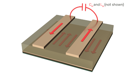
Electric current flowing through conductors creates electromagnetic fields with fascinating properties. Differential pairs showcase field interactions, and the two traces generate electromagnetic fields of equal magnitude but opposite polarity. This precise opposition enables mutual field cancellation when traces maintain close coupling.
Coupling
Coupling in a differential pair on a PCB refers to the close physical proximity and consistent routing of two complementary signal traces. This ensures they maintain equal impedance and reduce noise by allowing electromagnetic interference to affect both lines equally and cancel out.
--
The field cancellation power grows stronger as differential signals achieve tighter coupling. Closely spaced traces allow their opposing magnetic fields to neutralize each other, dramatically reducing radiated field energy. This mirrors the proven technique used in twisted pair cables, where conductor twisting ensures balanced interference exposure that differential receivers can easily filter out.
Odd and Even Mode Signal Propagation
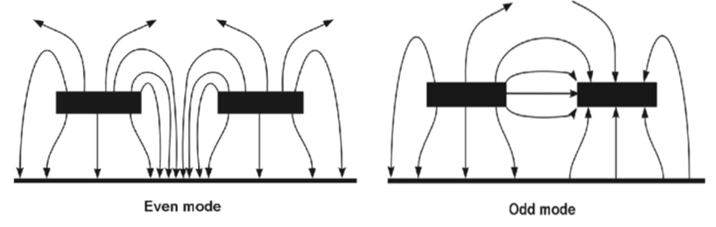
Image Credit: Polar Instruments - Even and Odd Mode Impedance [1]
Two distinct propagation modes define differential pair behavior:
- Odd mode: The desired state where lines carry equal but opposite voltages, creating differential signals. Each transmission line experiences a characteristic odd mode impedance.
- Even mode: An undesired state with signals matching amplitude and polarity, representing common-mode behavior. The associated impedance becomes even mode impedance.
Odd mode carries the intended differential signals, while even mode typically indicates unwanted noise. The beauty of odd mode operation emerges as equal but opposite currents flow, eliminating the return path current. This grants differential pairs excellent immunity to ground noise and reference plane variations.
Mathematical Models of Differential Pair
The mathematics reveals elegant relationships between impedance types. Differential impedance (Zdiff) equals twice the odd mode impedance (Zodd): Zdiff = 2 × Zodd. Similarly, common-mode impedance (Zcomm) equals half the even-mode impedance (Zeven): Zcomm = Zeven/2.
Mutual coupling between traces influences odd-mode impedance, keeping it below single-ended impedance values. Even-mode impedance demonstrates opposite behavior, exceeding single-ended impedance and increasing with stronger trace coupling.
For lossless transmission lines, odd-mode characteristic impedance follows:
Zodd = √[(L0 - Lm)/(C0 + 2Cm)]
Where L0 represents self-inductance, Lm mutual inductance, C0 self-capacitance, and Cm mutual capacitance per unit length.
Differential Pair Architecture in Modern PCBs
PCB designs demand sophisticated differential signaling solutions to power today's high-speed data transmission needs. Through careful architectural implementation, these paired traces showcase remarkable signal integrity capabilities.
Evolution of Differential Pair Technology
The PCB industry witnessed differential signaling mature from specialized applications into the cornerstone of high-speed digital design. Design teams discovered superior noise immunity, minimal EMI emissions, and exceptional signal integrity. Early implementations demanded meticulous manual adjustments for length matching and impedance control. Modern CAD tools now automate these requirements through intelligent design rules. Rising data speeds emphasize precise impedance control - boards must maintain 100Ω ±15% differential impedance.
Differential Pairs in High-Speed Protocols
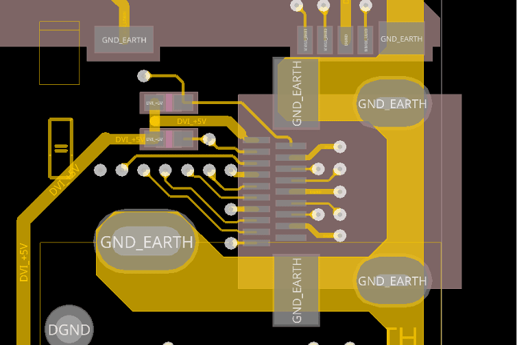
"When implementing a through-hole receptacle (like a USB Standard-A), TI recommends making high-speed differential signal connections to the receptacle on the bottom layer of the PCB. Making these connections on the bottom layer of the PCB prevents the through-hole pin from acting as a stub in the transmission path." - Texas Instruments Design Team, Semiconductor and PCB Design Experts
High-speed protocols push differential pairs to their limits, each demanding unique implementation strategies. These technical requirements ensure flawless data transmission across diverse operating conditions. Let's take a closer look at some of the most widely used high-speed protocols-USB, HDMI, DisplayPort, PCIe, NVMe, and Ethernet-and the specific design constraints that keep them performing at their best.
USB Implementation Requirements
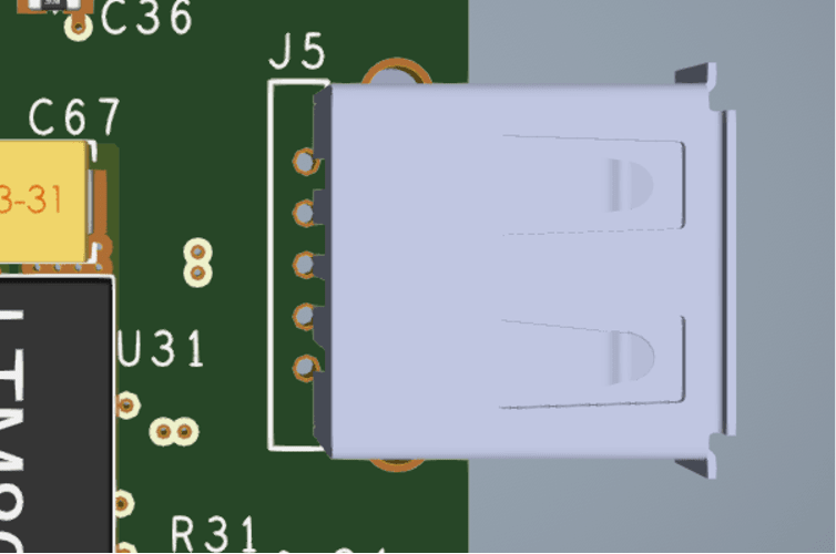
USB designs call for precise 90 ohm differential impedance, setting them apart from other protocols. D+ and D- traces perform best with minimal separation, typically 4-5 mils. Signal timing remains critical - skew must stay under 400 ps, equivalent to a 60 mm trace difference. High-speed USB routes demand clean paths without test points. When components prove necessary, 0402 or smaller packages minimize impedance disruptions.
HDMI and DisplayPort Routing Challenges
HDMI signals demand exactness - 100Ω ±5% differential impedance across Transition Minimized Differential Signaling (TMDS) pairs. Length matching rules tighten significantly compared to USB, requiring ±3mm matching between TMDS signals. DisplayPort pushes boundaries with 17.28 Gbps speeds, sharing architectural similarities with Ethernet and PCIe. Both protocols shine with strategic ground via placement near signal transitions.
PCIe and NVMe Differential Pair Specifications
PCIe architecture employs dual simplex channels, dedicating two differential pairs per lane. Four signal traces compose each lane - two receiving, two transmitting. Modern PCIe eliminates timing skew through embedded clock data. Success depends on maintaining 5W spacing between pairs while limiting via stubs to 15 mils.
Ethernet Differential Pair Design Considerations
Ethernet pairs thrive with 100Ω ±10% impedance control. Length matching varies by speed - 20 mils for 1G, 50 mils for 100M/10M. MDI traces perform optimally under 2 inches. Design rules mandate a 30 mil minimum pair separation and uninterrupted ground planes, except beneath specific components.
Looking Ahead
Future electronic designs will push differential pairs into new territory as data rates climb and form factors shrink. Their unmatched ability to preserve signal integrity while controlling electromagnetic interference positions them perfectly for next-generation computing and telecommunications advances. PCB designers who master differential pair implementation are key to unlocking tomorrow's high-speed digital systems.