How to Avoid Common PCB Design Mistakes
Key Takeaways
-
Common PCB design mistakes often occur in library management, schematic capture, physical layout (spacing, routing, vias, return paths), and BOM/manufacturing data generation.
-
OrCAD X mitigates these errors through integrated features like Component Explorer with verified libraries, ERC, a unified Constraint Manager with real-time DRC, and 3D visualization.
-
Live BOM in OrCAD X is critical for preventing component selection mistakes by directly providing real-time availability, lifecycle status, and pricing data within the design environment.
Designing a PCB involves numerous steps, from selecting components and capturing the schematic to routing traces and preparing for manufacturing. Along the way, common PCB design mistakes can range from minor annoyances causing extra rework to critical failures rendering a board unusable, costing valuable time and money. Fortunately, modern design tools like OrCAD X provide integrated features to help engineers catch and prevent these errors early. This article highlights frequent mistakes and demonstrates how leveraging OrCAD X capabilities can produce more manufacturable designs.
Common PCB Design Mistakes and OrCAD X Solutions
|
Mistake Category |
Common Examples |
OrCAD X Solution(s) |
|
Library & Components |
|
|
|
Schematic Design |
|
|
|
Layout & Routing |
|
|
|
BOM & Manufacturing |
|
|
Mistake #1: Library and Component Errors
The foundation of any PCB design lies in its component libraries. Errors here propagate throughout the entire project.
-
Incorrect Footprints: Perhaps the most frequent library mistake is using a footprint that doesn't precisely match the physical component. This error leads to assembly problems, where parts simply won't fit on the pads, requiring board respins.
-
Wrong Schematic Symbol: Selecting a symbol that doesn't accurately represent the pinout or function of the chosen part guarantees incorrect connectivity in the schematic.
-
Using Obsolete or Unavailable Parts: Choosing components without verifying their lifecycle status or current availability can halt production when part sourcing fails, leading to invalid BOM creation.
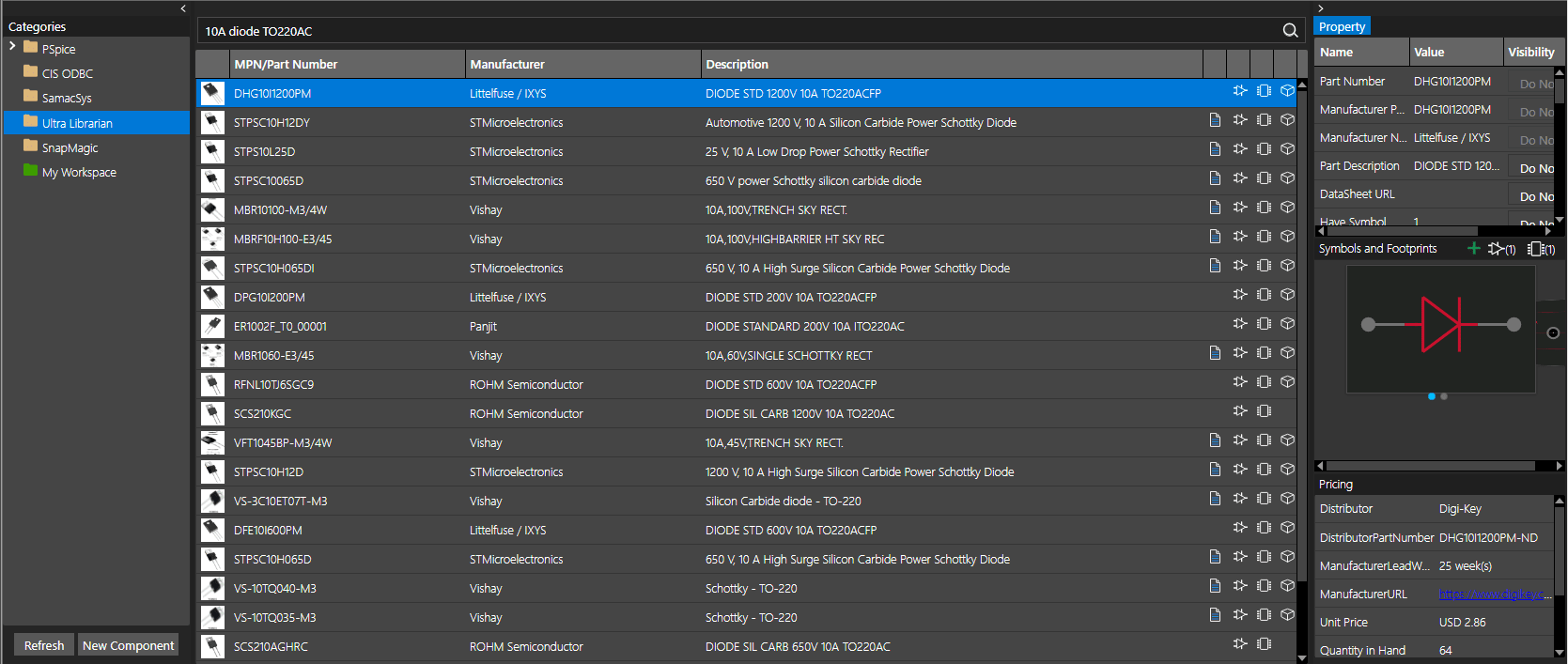
OrCAD X provides several features to mitigate these library-related errors. With the Component Explorer, engineers can link verified schematic symbols, PCB footprints, and 3D models to a single component definition stored centrally. Additionally, the Component Explorer integrates directly with major suppliers like Ultra Librarian, SamacSys, and SnapMagic, providing access to millions of pre-built, verified library parts, including parametric data, and significantly reducing manual footprint creation errors.
Mistake #2: Schematic Design Oversights
The schematic captures the logical intent of the circuit. Errors here often lead to functional failures.
-
Connectivity Errors: Unconnected pins (floating inputs), missing net connections, or nets incorrectly shorted together are common oversights.
-
Missing Decoupling Capacitors: Forgetting to place appropriate decoupling capacitors near IC power pins can lead to noise issues and unstable operation.
-
Incorrect Component Values/Types: Specifying the wrong resistance, capacitance, or component type (e.g., electrolytic vs. ceramic capacitor) can prevent the circuit from functioning as intended.
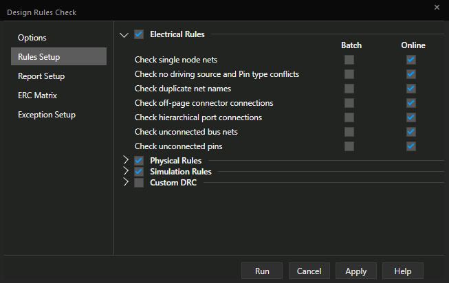
To catch these schematic issues, OrCAD X Capture includes Electrical Rules Check (ERC) capabilities, which analyze the schematic for common errors, flagging potential problems before layout begins. Furthermore, easy net highlighting allows tracing connectivity across complex, multi-sheet schematics. At the same time, cross-probing enables instant navigation between a selected schematic element and its corresponding representation in the PCB layout, aiding verification.
Mistake #3: Layout and Routing Issues
Translating the schematic to the physical layout introduces a new set of potential errors related to physical implementation. Insufficient attention to detail can compromise manufacturability, signal integrity, and overall performance.
Common Layout and Routing Mistakes
|
Layout Issue |
Common Mistake |
Consequence |
Recommended Solution |
|
Insufficient Trace Spacing |
Use only minimum manufacturable spacing, especially for long parallel runs. |
Increased crosstalk, noise, and reduced manufacturing yield. |
Employ wider spacing (e.g., >= 3x dielectric height between trace and reference plane). Minimize the length of parallel runs where possible. |
|
Inappropriate Trace Widths |
Applying a single default width to all signals. |
Insufficient current capacity/voltage drop on power traces; impedance mismatch on high-speed lines. |
Size widths depend on function: They are wider for power, calculated for controlled impedance, and potentially thinner for high-impedance analog signals. |
|
Improper Via Sizing |
Specifying drill diameters or annular rings smaller than the manufacturer's minimums; using unnecessarily large vias. |
Via breakout, open circuits, wasted board space, and potential manufacturing failures. |
Use appropriate via sizes (e.g., 0.7mm pad/0.3mm drill standard). Ensure the minimum annular ring meets requirements. Size/duplicate vias based on current needs (e.g., power). |
|
Signal Return Paths & Planes |
Routing high-speed or sensitive signals across splits or voids in their adjacent reference plane. |
Forces long, inductive return current loops, causing significant noise, crosstalk, and EMI issues. |
Use solid, uninterrupted reference planes adjacent to signal layers. Never route critical signals across plane splits. Ensure return path continuity during layer changes (stitching vias). |
|
Other Common Layout Issues |
Poor grounding strategies, signal integrity violations (stubs, impedance mismatches), acid traps, and inadequate thermal management. |
Noise susceptibility, signal degradation, manufacturing defects (shorts/opens), and component overheating. |
Follow established best practices for grounding, high-speed design, DFM (avoid acute angles), and thermal considerations for power components. |
OrCAD X provides a comprehensive suite of tools to prevent these physical design errors. The unified Constraint Manager is central, allowing the definition of detailed electrical and physical (spacing, width, via types), and manufacturing rules applied directly to the layout. Real-time Design Rule Check (DRC) gives immediate feedback on violations during layout. The padstack editor ensures consistent use of correctly defined vias.
For return path management, the layer stackup manager helps define layer structure, while plane generation tools and 3D visualization capabilities allow easy creation and inspection of solid reference planes, helping identify traces crossing splits. Cross-probing aids in understanding the physical routing relative to schematic intent and reference planes. Furthermore, integration with Sigrity X allows for detailed signal, power, and thermal analysis, or PSpice for circuit simulation, to identify issues before fabrication.
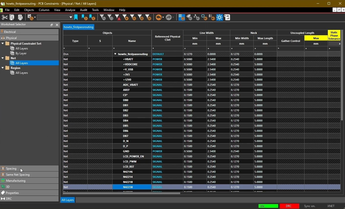
The OrCAD X Constraint Manager displays physical constraints set for all nets in the design.
Mistake #4: BOM Errors and Poor Component Selection
Errors in the Bill of Materials (BOM) or selecting inappropriate components are quite common PCB design mistakes that directly impact cost, manufacturability, and project timelines. Key pitfalls include incorrect Manufacturer Part Numbers (MPNs), linking the wrong footprints, using obsolete or unavailable parts discovered only at the procurement stage, and simple quantity or description errors.
With Live BOM, OrCAD X offers robust solutions to prevent these critical issues. The Component Information System (CIS) acts as a central database, ensuring that verified MPNs, descriptions, values, and footprints are consistently linked and used for BOM generation. Live BOM feature elevates this by integrating directly with supplier databases, allowing real-time verification of component pricing data, availability, and lifecycle status (Active, NRFND, Obsolete) directly within the OrCAD X environment during design. Finally, automated BOM generation pulls data directly from the verified design database, reducing manual counting errors and ensuring accuracy, with customizable templates available for specific formatting needs.
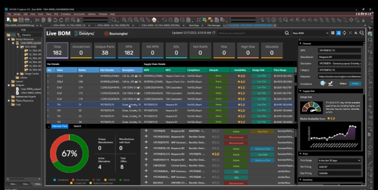
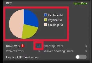
The Live BOM Dashboard in OrCAD X provides a risk profile of its components.
Navigating the complexities of board layout requires vigilance to avoid common PCB design mistakes. OrCAD X provides an integrated suite of tools designed to catch errors early, from schematic inconsistencies identified by ERC to layout violations flagged by real-time DRC and the Constraint Manager to sourcing issues prevented by Live BOM. Leverage these preventative capabilities to ensure your next project is robust and manufacturable. Try OrCAD X for free and explore the complete OrCAD X platform to see how it can streamline your workflow and help you design more confidently.
Leading electronics providers rely on Cadence products to optimize power, space, and energy needs for a wide variety of market applications. To learn more about our innovative solutions, subscribe to our newsletter or our YouTube channel.