Impedance Analysis Workflow Using Sigrity X Aurora in PCB Layout
Purpose
This document provides the step-by-step procedure on performing Impedance Analysis within the PCB layout canvas for quick identification of impedance discontinuities and to identify if the impedance meets the defined constraints.
Audience
This RAK is intended for PCB layout engineers and Signal Integrity engineers.
Overview
The Sigrity technology-driven high-speed analysis and checking environment provides analysis and checking capability within the Allegro PCB Editor framework. Multiple workflows are available in Sigrity Aurora: Impedance, Coupling, Crosstalk, Reflection, Return Path, and IR Drop. In this RAK, the Impedance Workflow is covered.
Download
The RAK database and references can be found in the ‘Attachments’ and ‘Related Solutions’ sections below the PDF. This RAK pdf can be searched with the document title on https://support.cadence.com.
License Requirement
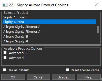
Sigrity Aurora is the preferred license for this RAK, offering the analysis workflows in Allegro PCB Editor.
Terms
| CM | Constraint Manager |
| IDA | In-Design Analysis |
| PCB | Printed Circuit Board |
| Diff Pair | Differential Pair |
Module 1: Impedance Constraint in Constraint Manager
Impedance Constraints
You can use Constraint Manager to identify problems in impedance by placing DRC on the nets that present impedances outside the acceptable range.
-
Launch Allegro X PCB Editor (OrCAD X support coming in release 25.1 (Oct 2025)) and select the Sigrity Aurora license.
-
Open the brain_board.brd design file.
-
Open Constraint Manager by using Setup > Constraints > Constraint Manager from the top menu or by clicking on the Constraint Manager icon in the top menu bar.

-
On the left side, use the Worksheet selector and navigate to Electrical > Net > Routing > Impedance.
-
Search for the P0_USB_D bus. You can do it by scrolling the list or by typing its name in the Name search filed.
-
In the Single-line Impedance column, assign the target impedance to 45 Ohm and the tolerance to 5%.

Note that many DRCs appeared in the top layer of the design. This impedance DRC check is quite useful to help identify the nets that do not have impedance values within the specified range.

This DRC check cannot help identify the exact points where the mismatch happens. Impedance Workflow in the Sigrity Aurora is a powerful tool that fills this gap.
-
Clear the constraints assigned to the P0_USB_D bus to remove the DRCs.
Module 2: Impedance Workflow
Impedance Analysis Setup
-
Launch Allegro X PCB Editor (OrCAD X support coming in release 25.1 (Oct 2025)) and select the Sigrity Aurora license.
-
Open the brain_board.brd design file.
-
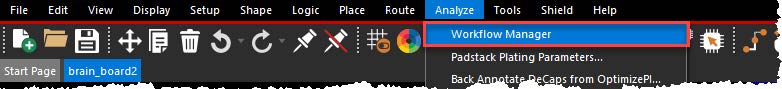
In the top menu, select Analyze > Workflow Manager.
-
Select Impedance Workflow in the Analysis Workflows pane.
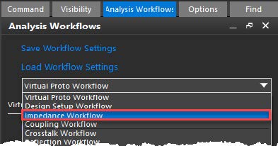
Note that the necessary steps are indicated with a red X and various links are disabled until those required steps have been completed.
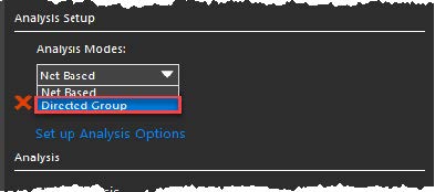
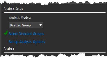
There are two ways to set up Analysis: Net Based and Directed Group. In a Net Based analysis, every segment of the selected nets is simulated, whereas in a Directed Group analysis, only the net portions specified by a start component and one or more end components are simulated.
-
Choose Directed Group from the dropdown menu.
-
Select the Select Directed Groups link in the workflow.
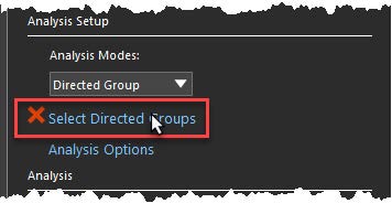
This link is used to create and select the active directed group.
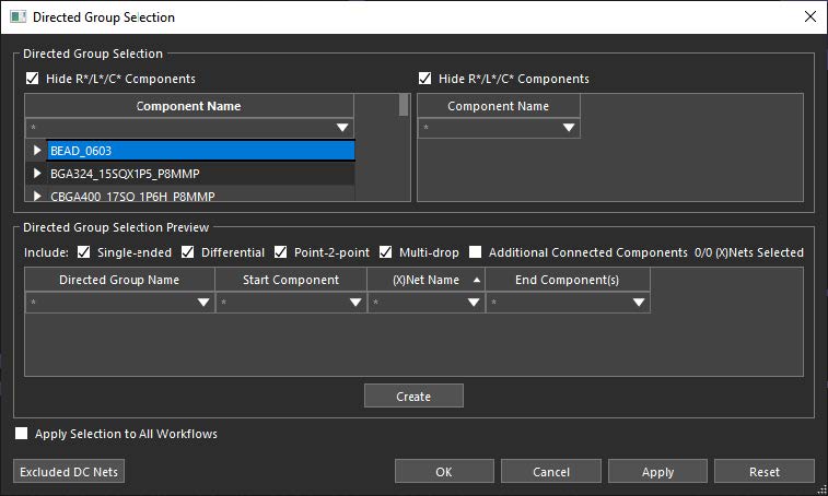
Most of the dialog is dedicated to creation. Directed Groups (as a method) can be thought of as component-based net selection and as the name implies, you indicate directionality by selecting the Start and End components.
-
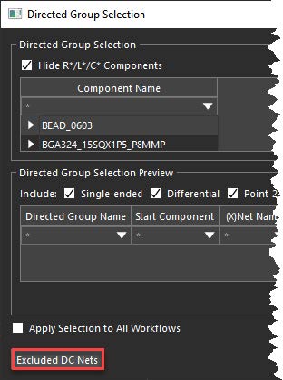
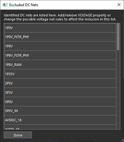
Select the Excluded DC Nets button. As the dialog explains, these are the currently defined Voltage nets in the design.
-
Click Done in the Excluded DC Nets dialog.
-
In the canvas, search and click U12 first and then U2.
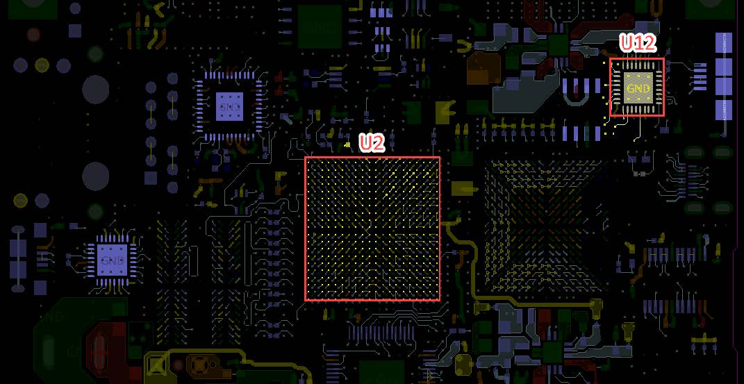
Note that U12 and U2 are now selected as the start and end components, respectively. This state can also be achieved by typing U12 in the left search bar, U2 in the right search bar, and marking the checkboxes. It is also possible to use the Hide R*/L*/C* Components option and wildcards to help filter items.
-
Make sure that all necessary direct group net boxes are selected and click the Create button.
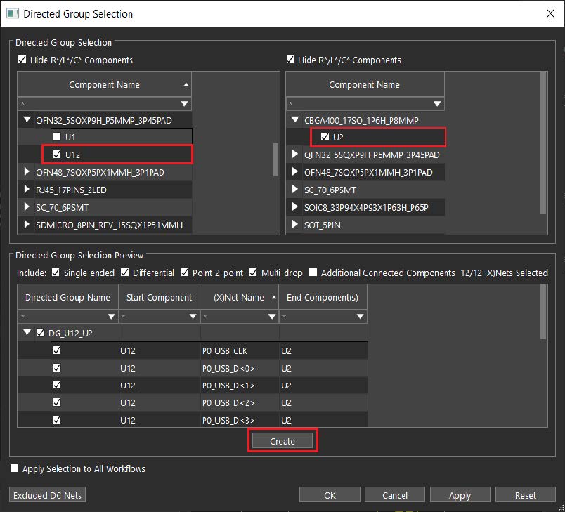
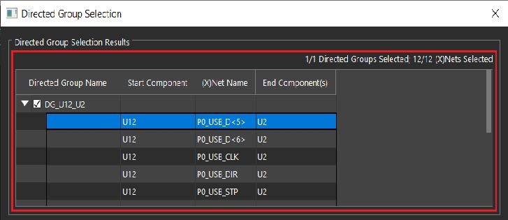
This will create one directed group with a total of 12 (X)Nets, which will be shown on the top of the dialog box.
-
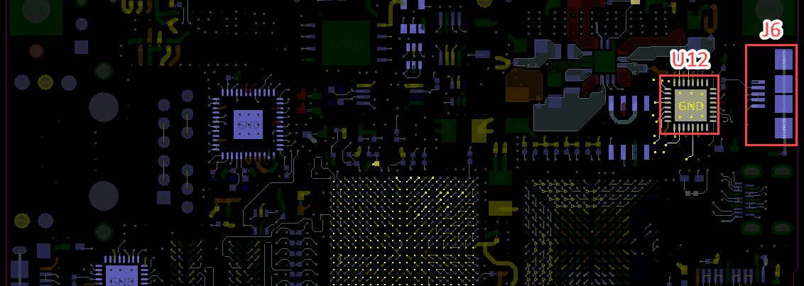
Return to the canvas and first select J6 and then U12.
-
Unselect P0_USB_ID >> P0_USB_ID_X and P0_VBUS >> N21090237 (X)Net names and click Create. This will create another directed group, increasing the total of (X)Nets to 14.
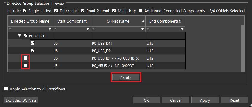
Notice that there is now a green checkmark next to Select Directed Groups and that the Start Analysis link is now active.
-
Select the Set up Analysis Options link, right below the Select Directed Groups link.
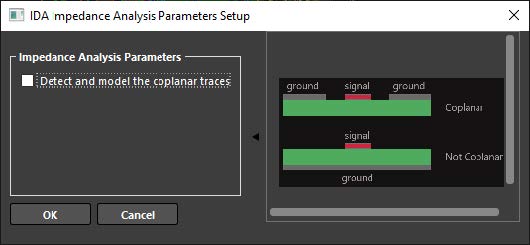
There is only one option, Detect and model the coplanar traces, here. If you do not have coplanar structures in your design, you do not need to enable this.
-
Click Cancel in the IDA Impedance Analysis Parameters Setup dialog.
-
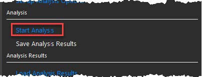
Click on the Start Analysis link in the workflow and wait until the simulation is done.
Simulation Results
-
Once the analysis is complete, select Directed Group and Single Ended in the View Modes settings.
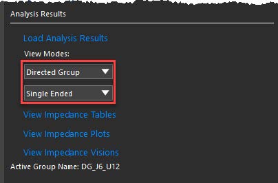
Note that the View Impedance Plots link is now available and that the active group is listed. Plots use the distance from the starting component on the X-axis, and hence, are only available when Directed Group is selected in View Modes.
-
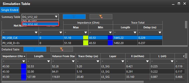
Select View Impedance Tables in the workflow. You will get a dockable Simulation Table window as shown below.
-
Make sure that the direct group selected is DG_U12_U2.
-
Search and select the P0_USB_CLK net in Summary Table (top half). This will update Detailed Table (bottom half) with the impedance of each segment of the net.
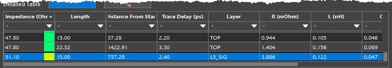
-
Search for the segment with the highest impedance and double-click it. The segment will be focused on the canvas. It also automatically enables the layer where the segment is, in this case, the L2_Sig layer.
-
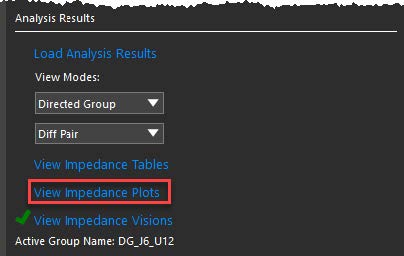
Select View Impedance Visions in the workflow.
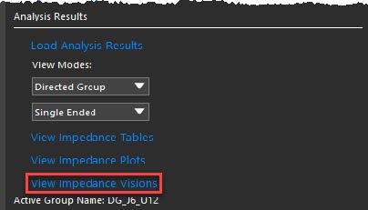
Overlays that were previously available only in the side-by-side configuration with ERC are now available directly in the Allegro canvas. The overlays are using the same “vision” concept that was introduced with Timing Vision. These new analysis visions provide a quick-and-easy way to get a global view of what was just analyzed.
-
Zoom out a bit to have a better vision on the nets connecting U12 and U2.
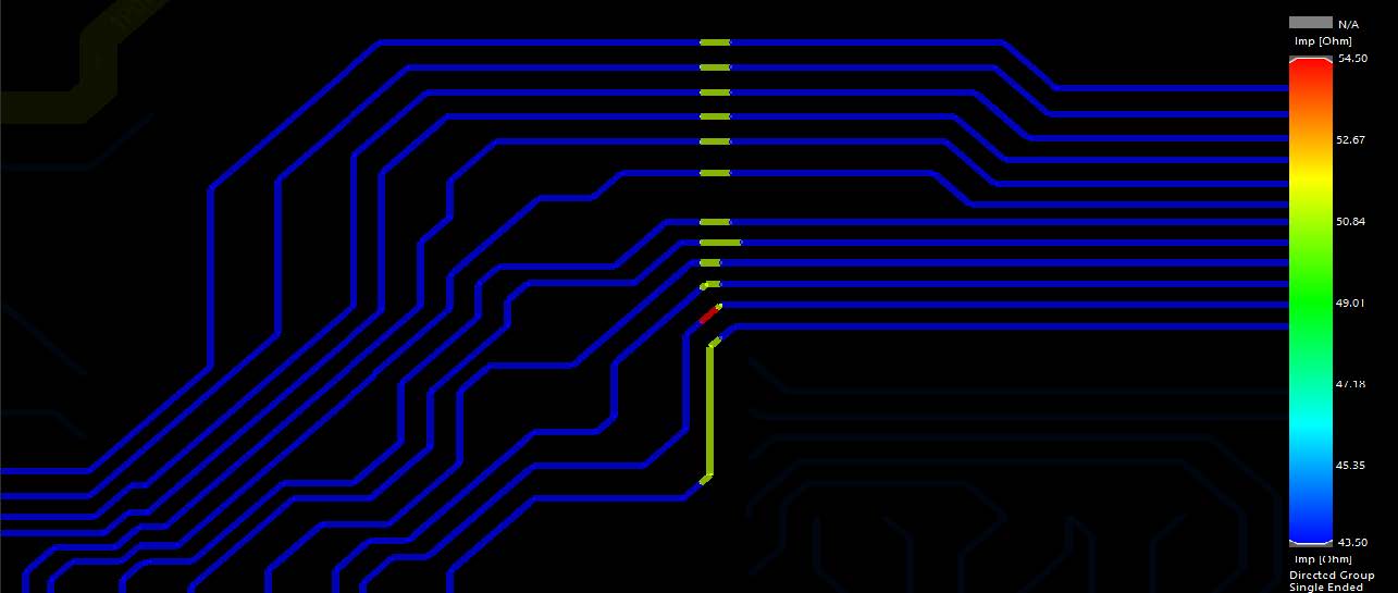
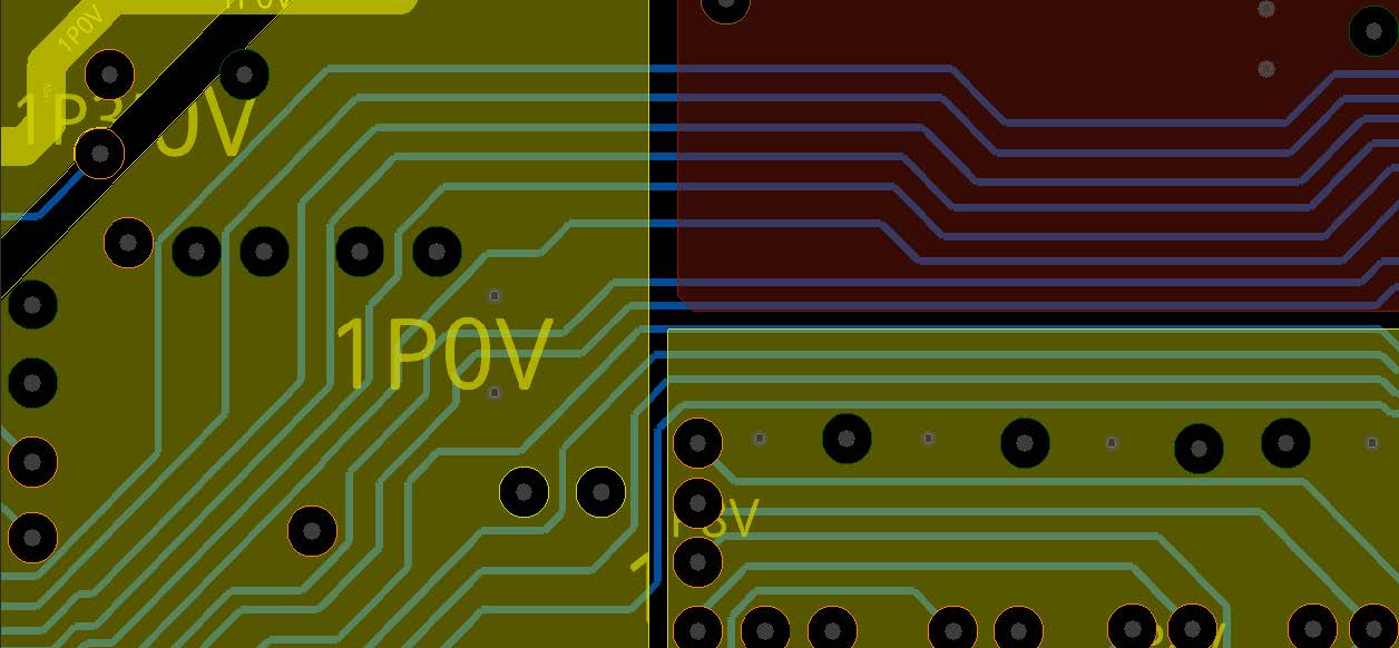
Notice that there is an area where the impedance value increases. This happens because there is a plane discontinuity in the L6_Pwr layer, which is an adjacent layer. This can be seen by disabling Impedance Vision and enabling the visibility of L5_Sig and L6_Pwr layers.
If necessary, sliders on the color gradient can be used to filter impedance values. Also note the grey color at the top, which indicates traces with no reference found in the stackup.
-
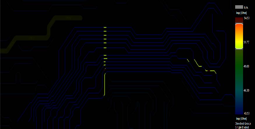
Return to the Simulation Table window and change the direct group to DG_J6_U12.
-
Toggle the Single Ended pulldown to Diff Pair. This is the same data with differential pairs color coded. Note that the gradient has adjusted on the high end to account for differential impedance values, and that the nets previously visible are not being shown anymore. This happens because the nets shown here are only differential pairs, which are not in the L5_Sig layer. These are on the L3_Sign layer.
-
Select View Impedance Plots from the workflow. Make sure that the Bar/Expanded tab is selected.
Note that the label on the X-axis is for Distance From Start. Some important features in the plot are tooltips, cross-probing to the Allegro canvas, and the ability to filter by making selections in the Net Name pane.
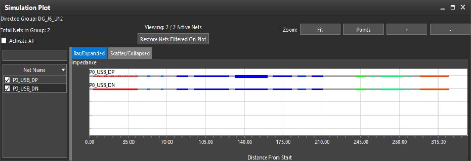
Note: If the plot is empty or not all active nets are being shown, select the Restore Nets Filtered On Plot button to reset the display.
-
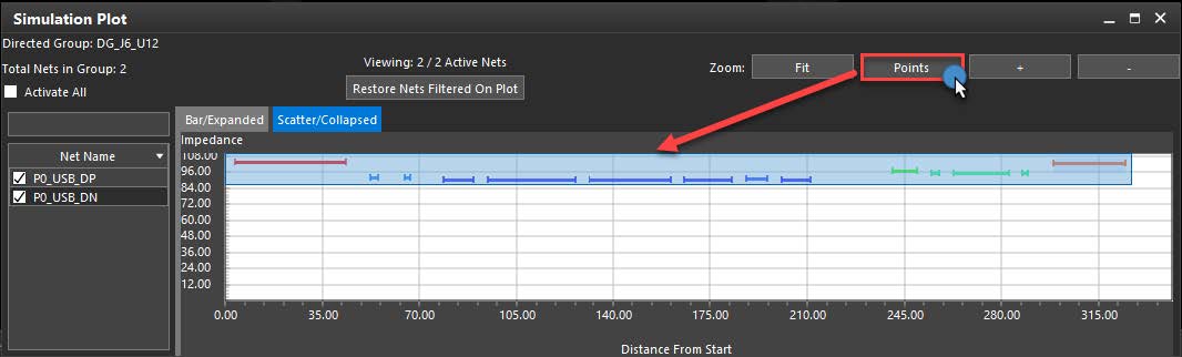
Select the Scatter/Collapsed tab in the Simulation Plot pane ( use Activate all if necessary). This plot provides a better global view of the entire design.
-
You can use the Fit button to make the plot fit or use the Points button of the Zoom section and drag a window around the area indicated in the following box.
-
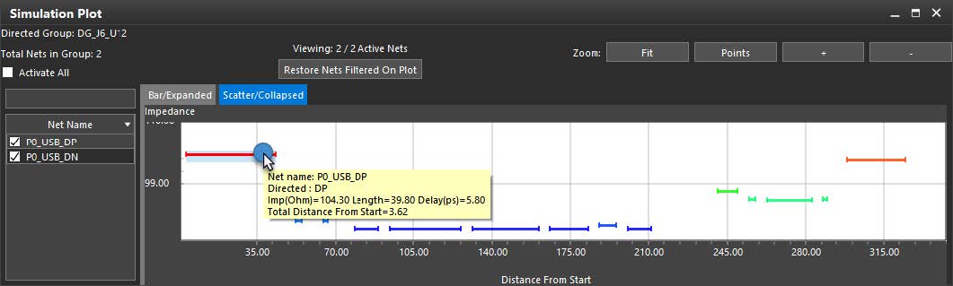
Click on the top-left segment, which is the one with the highest impedance. The segment will be focused on the canvas.
-
Make sure that both Top and L3_Sig layers are enabled, so it is possible to see the complete circuit.
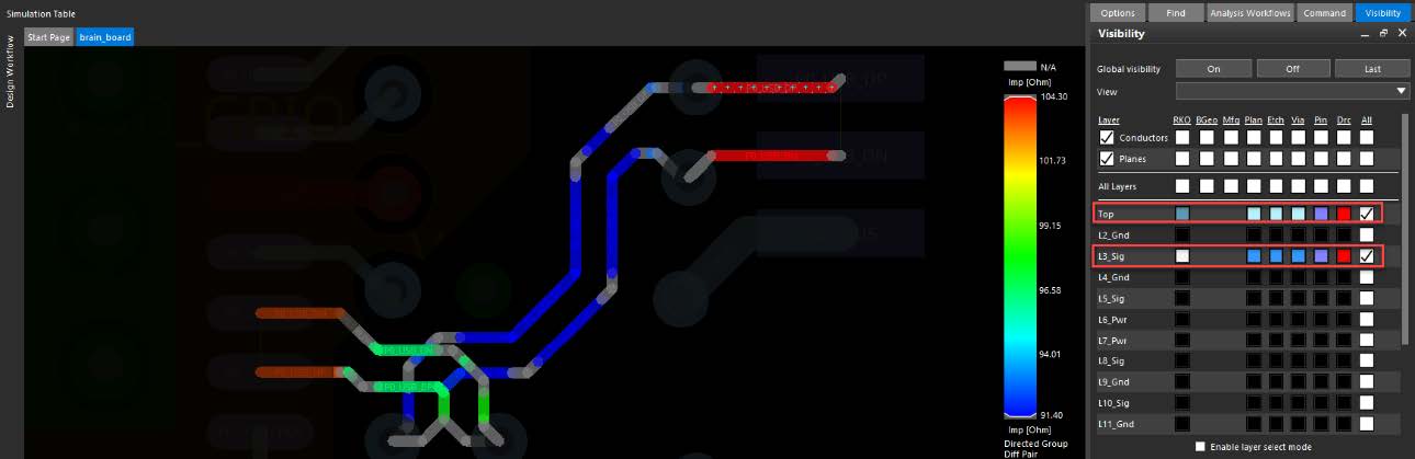
The differential pair impedance depends on the distance between the nets, besides other parameters, such as trace width, dielectric constant, and distance from the reference planes.
-
Reduce the space between the nets with the highest impedance and simulate the board again to see the impedance value reduce.
-
If necessary, these same nets can be analyzed as single-ended by just switching from Diff Pair back to Single Ended. Note that Impedance Analysis in Sigrity Aurora is targeting the trace impedance. Via parasitics are not reported. Aurora includes the Reflection and Crosstalk flows, which does include via parasitics in simulations if you need this data extracted. For the Return Path check, Impedance Analysis in Aurora provides the checking for trace reference planes.
This completes the RAK.
Support
Cadence Learning and Support Portal provides access to support resources, including an extensive knowledge base, access to software updates for Cadence products, and the ability to interact with Cadence Customer Support. Visit https://support.cadence.com.
Feedback
Email comments, questions, and suggestions to content_feedback@cadence.com.
Attachement
RAK_Database_Analysis_impedance.zip
If you have any questions or comments about the OrCAD X platform, click on the link below.
Contact Us