Circuit Board 4-Layer PCB Stackup Planning
Key Takeaways
-
Understanding the requirements of a 4-layer printed circuit board
-
Design recommendations for a 4-layer PCB stackup
-
Using your design tools in a 4-layer PCB design
It is fascinating to watch a skilled cook combine different items, sauces, and seasonings to create a culinary masterpiece. But, could you imagine if they were only allowed to work with four ingredients? How much could they do with restrictions like that? Believe it or not, circuit board designers do it all the time with just four layers in a circuit board.
Four layers in a circuit board will reduce many manufacturing expenses and are therefore a popular choice for consumer electronics. However, designing with only four layers poses some unique challenges in satisfying the board’s routing and signal integrity requirements. Creating a restrictive design that checks all the boxes for size, cost, manufacturability, and electrical performance starts with configuring the layer stackup. This article will share some information and recommendations on the 4-layer PCB stackup to help you get started.
PCB Layer Configuration Strategies
There are many ways to design and build a circuit board. Although FR-4 is a standard material group for use as the PCB substrate, there are plenty of other materials as well. Circuit boards are typically built using a subtractive process of etching away unwanted copper, but additive processes are gaining popularity. And, of course, the number of layers used in a circuit board can vary from a single or double-sided board to a multi-board configuration with four, six, eight, or more layers in it.
Determining the manufacturing process, materials, and layer configuration all boils down to performance and cost. Obviously, we want the circuit board to have the best performance while at the same time costing as little as possible to produce it. However, each of those factors has a great amount of influence over the other. High-density, high-speed designs with thousands of interconnects on them are simply not going to fit on a double-sided board, nor will the board’s configuration support the performance of the electronics. While laying out a ten-layer board gives the designer an ample amount of space for a simple design, it just doesn’t make sense to pay for that many layers if fewer will work.
It is up to the design team to come up with the best PCB layer configuration strategy for their design and, in many cases, a 4-layer circuit board will do the job. However, there are many aspects of the 4-layer circuit board that must be considered, starting with understanding all of what will be required of the circuit board.
4-layer PCB layouts require tight component placement and routing
Understanding the Requirements
To accurately plan the configuration of the board, you first have to understand all it will be expected to do, starting with its physical requirements:
-
Purpose: What environment the board will be expected to operate in will have a huge bearing on how it will be built. Extreme temperatures or high-moisture environments may require a change in the materials used for fabricating the board, altering how it will be designed.
-
Size and shape: Depending on where the board will be installed, the size and shape may require a change in board layers to accommodate all of its trace routing. The size and shape could also impact how the board will be manufactured.
-
Technology: The type of components and speed of the circuitry will also affect how the layer stackup of the board will be configured. The routing requirements of large, high-density parts like BGA footprints may require additional layers to route out of all of its pins.
-
Features: Holes, brackets, cut-outs, and other unique features could also impact how many layers the board needs.
Another aspect of evaluating the circuit board’s requirements is understanding its electrical and performance expectations:
-
Signal integrity: Depending on the technology type, there may be design requirements for controlled impedance routing and EMI shielding, increasing the number of ground plane and routing layers.
-
Power integrity: Depending on the power requirements, more layers may be required to build a robust power delivery network on the board.
Ultimately, three main requirements have to be met in the production of a circuit board. It is up to the design team to determine if a 4-layer configuration will satisfy these requirements.
-
Is It Manufacturable?
Reducing the trace widths and clearances to fit them into fewer layers may make the board too difficult to build without paying a significant penalty in manufacturing time expense.
-
Is It on Time and Within Budget?
The cost increase between building a four and six-layer board can be as much as 30 to 40 percent. This increase is a great incentive to keep the layer count down in the design as long as it is manufacturable.
-
Will It Meet Its Performance Specifications?
The board must perform according to its operating specifications, even if configuration changes are required to accomplish this.
Assuming that all of these requirements can be met with a 4-layer design, let’s look at what is involved.
Another useful feature in 4-layer PCB stackup layout is controlling the design rules of part placement
The 4-Layer PCB Stackup
Laying out a 4-layer printed circuit board can be a real challenge to designers who are used to having more space available to them. Instead of having layers devoted to routing, they may end up sharing space with copper pours and wide traces for power delivery. Here are some specific design considerations to keep in mind for a 4-layer PCB stackup.
Grounding Is Essential
Circuit board signals, especially high-speed signals, must have a clear return path for the best signal integrity of the design. This requirement holds true for all signals, whether they are digital, analog, or power. To accommodate this means devoting one of the internal layers of the 4-layer board to a dedicated ground plane. With the outer layers of the board devoted to component placement and the remaining internal layer filled with signal and power routing, the design will rapidly run out of usable space. But, it is imperative that the ground plane not be split to provide a clear return path to reduce or eliminate EMI in the design.
Power Delivery
Many components used in today’s designs have different voltage level requirements. These power requirements can create a challenge for the designer to route all of these voltages on a 4-layer board while maintaining a clean power delivery system. Usually, designers will route power with a combination of split planes and wide traces. Additionally, the placement and routing of bypass caps must be factored in to ensure that they have the shortest and most direct routing to their assigned supply pins.
Escape Routing
Here is where laying out a 4-layer circuit board can become very intricate. The more rows of pins on a large-scale BGA component, the more layers will be needed for the escape routing. While the outer rows of the part can be routed out, the next rows will have to be connected through a via. A 4-layer board will eventually run out of layers to route out of a large device successfully.
Trace Routing
Mixed-signal designs are common today, and their routing rules need to be followed even on a smaller 4-layer board. A continual ground plane is essential for a mixed-signal design. Don’t route across breaks in the reference ground plane and keep digital and analog circuitry isolated from each other as much as possible. Remember that you probably won’t have a dedicated internal layer for routing, so routing must be planned along with component placement and escape routing to ensure there is adequate space for all.
Copper Balancing and Heat Dissipation
To maintain the symmetry of the board for fabrication and assembly, using an internal power plane to offset the internal ground plane is a good idea. However, with the need for a routing layer, you may be forced to combine split power planes or wide traces with regular signal routing. Thermal balancing can be done with ground vias transferring the heat of large components down through the ground plane.
To keep track of all the requirements necessary to lay out a successful 4-layer circuit board, you need to leverage the full functionality of your PCB design tools. Next, we’ll look at some of the tool features and functionalities that can be the most helpful.
Cadence’s Cross-Section Editor in their Allegro PCB Editor design tools
Using the Full Power of Your PCB Design System
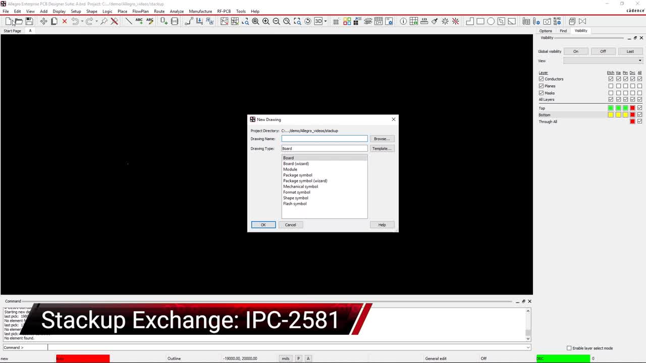
One of the big advantages to PCB designers today is the ability to work together with their manufacturers on the best configuration of their circuit boards. Cadence has helped this relationship with their IPC-2581 capabilities, as shown in the video at the top of this article. This feature allows designers to receive stackup information from their manufacturers and import the data directly into Cadence’s Cross-Section Editor. After configuring the board, the stackup can be sent back to the manufacturer for confirmation and stored externally for use in future designs.
However, the Cross-Section Editor is more than just a vessel for external data. Cadence Allegro uses this editor to create and modify the board layer stackup in a PCB design. In the image above, you can see the configuration of a typical 4-layer PCB stackup in circuit board design, with the ability to specify routing layers, top, bottom, and plane layers, plus much more.
For more information on PCB stackup strategies, especially in calculating the cost, take a look at this E-book from Cadence.
If you’re looking to learn more about how Cadence has the solution for you, talk to our team of experts.