Creating PCB Design Constraints in OrCAD X
Key Takeaways
-
OrCAD X organizes constraints into Electrical, Physical, Spacing, Manufacturing, and High-Speed categories for rule-based management.
-
Net Classes, Net Groups, and Regions help efficiently apply and manage constraints in specific areas or across grouped nets.
-
How to set up different types of constraints in OrCAD X.
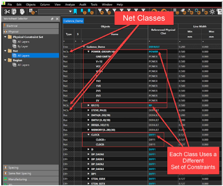
OrCAD X constraint manager with net classes and associated applied rules.
Constraint management in PCB design involves defining and enforcing specific rules to ensure a design meets performance, manufacturability, and reliability requirements. These constraints govern aspects like:
-
signal integrity,
-
component placement,
-
spacing,
-
and manufacturing tolerances.
By systematically applying constraints during the design phase, engineers mitigate errors early, optimize performance, and ensure compliance with manufacturing standards. This structured approach reduces design iterations, enhances reliability, and streamlines complex PCB development processes.
In OrCAD X, constraints are organized into types: Electrical, Physical, Spacing, Manufacturing, and High-Speed Design Constraints. Creating PCB design constraints is accomplished through the Constraint Manager (CM).
Access the CM Located under Tools > Constraint Manager in OrCAD X Presto PCB Editor.
Creating PCB Design Constraints — Capabilities
|
Constraint Type |
Applications and Benefits |
Capabilities |
Example |
|
Electrical Constraints |
- Ensures signal integrity and timing accuracy. - Prevents degradation and EMI issues. - Optimizes power delivery and return paths. |
- Propagation delay and timing control. - Impedance matching (single/differential pairs). - EMI control and crosstalk prevention. - Wiring topology settings. |
Matching differential pair lengths for USB signals. |
|
Physical Constraints |
- Controls physical layout and manufacturability. - Improves board design performance. - Supports component placement optimization. |
- Board outline and layer stack-up control. - Component placement rules. - Via type and differential pair geometry. - Trace width and neck-down rules. |
Defining 0.1mm trace widths for fine-pitch BGA regions. |
|
Spacing Constraints |
- Prevents electrical shorts and EMI. - Ensures mechanical and thermal reliability. - Reduces layout errors and enhances spacing compliance. |
- Trace-to-trace and trace-to-pad clearance. - Component-to-component spacing. - Conductor/via spacing. - Plane spacing and board edge rules. |
Setting 0.5mm clearance between high-voltage traces. |
|
Manufacturing Constraints |
- Ensures design compatibility with manufacturing processes. - Reduces fabrication errors and improves yield. - Lowers production costs. |
- Minimum trace width and spacing. - Drill sizes and tolerances. - Solder mask and silkscreen rules. - Copper pour and aspect ratio control. |
Specifying minimum drill size of 0.3mm for vias. |
|
High-Speed Design Constraints |
- Maintains performance of high-speed circuits. - Prevents signal reflection, skew, and crosstalk. - Ensures proper operation in high-frequency designs. |
- Length matching and impedance routing. - Skew tolerance and stub management. - Via stitching for return path optimization. - Crosstalk mitigation rules. |
Length matching for DDR memory data lines. |
|
Thermal Constraints |
- Prevents thermal damage and overheating. - Improves heat dissipation and reliability. - Reduces failure rates for heat-sensitive components. |
- Define component thermal zones. - Use via arrays for heat sinking. - Copper pour rules for better heat dissipation. |
Adding via stitching under power regulators for heat dissipation. |
|
Constraint Regions |
- Enables area-specific rules for complex designs. - Overrides global constraints in critical regions. - Allows tighter control in dense board areas. |
- Apply unique rules to regions. - Override global constraints selectively. - Define physical/spacing rules per region. |
Setting tighter trace widths in a BGA region for fine-pitch routing. |
How to create a net class in OrCAD X. For more detailed information, see the OrCAD X Constraint Management Guide.
Creating PCB Design Constraints: Set-Up
OrCAD X uses Net Classes, Net Groups, and Regions as tools to organize and manage design rules. We’ll dive into how to create each in the sections below.
Key Differences: Net Classes, Net Groups, and Regions
Creating PCB design constraints can be done for multiple domains using step-by-step methods. To begin, Net Classes allow designers to group nets and assign Physical Constraint Sets (CSet), simplifying the process of applying trace width or via rules across power or signal nets. Net Classes group nets that share similar properties, such as power or signal nets, allowing domain-specific rules like trace width or impedance to be applied collectively.
For broader organization, Net Groups are created to manage collections of nets with diverse properties but common functional needs. Designers can define Spacing Constraint Sets (SCS) for these groups to maintain consistent clearances across traces, vias, or components. Net Groups enable higher-level organization, spanning across multiple domains. They are ideal for managing nets with the same functional protocol but have varying physical or electrical properties. For instance, USB-related nets with different impedance requirements can still be grouped to apply general spacing rules.
For area-specific requirements, Regions are defined to override global rules in specific sections of the PCB. For example, in areas with fine-pitch BGAs, smaller trace widths and tighter spacing rules can be applied by creating both Physical and Spacing Constraint Sets. These sets are then assigned to the region, ensuring precise control without affecting the rest of the design. By combining classes, groups, and regions, constraints are applied efficiently, enabling organized rule management and quick updates when design changes occur.
-
Net Classes: Apply rules to groups of nets (domain-specific).
-
Net Groups: Organize nets across domains for generalized rule application.
-
Regions: Apply constraints to specific physical areas on the PCB, overriding global rules when necessary.
Setting Up Electrical Constraints
Electrical constraints focus on signal integrity, impedance control, and EMI management. Here’s how to create electrical constraints:
-
Open the Constraint Manager:
-
Go to Tools > Constraint Manager in OrCAD X Presto PCB Editor.
Set Electrical Constraint Sets (ECS):
-
Select the Electrical Constraints worksheet.
-
Define key parameters such as:
-
Impedance for traces (single-ended or differential pairs).
-
Signal timing for specific nets.
Apply the ECS to nets, net groups, or regions.
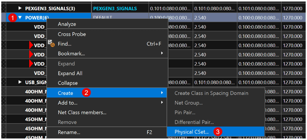
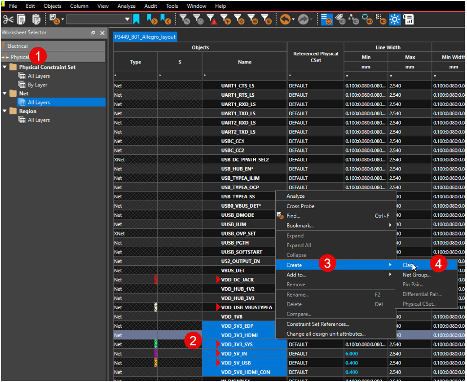
How to create a Physical CSet in OrCAD X. For more detailed information, see the OrCAD X Constraint Management Guide.
Setting Up Physical Constraints
Creating Physical constraints can ensure proper component placement, trace width, and via definitions.
Steps:
-
In CM, go to Physical Constraints.
-
Use Net Classes to group nets with shared physical properties:
-
Example: Assign power traces (e.g., VDD_5V) to a "Power" net class.
Apply a Physical Constraint Set:
-
Right-click the Net Class and select Create > Physical CSet.
-
Define parameters like minimum/maximum trace width and via usage.
Benefits: Changes to a CSet are automatically applied to all nets within the class.
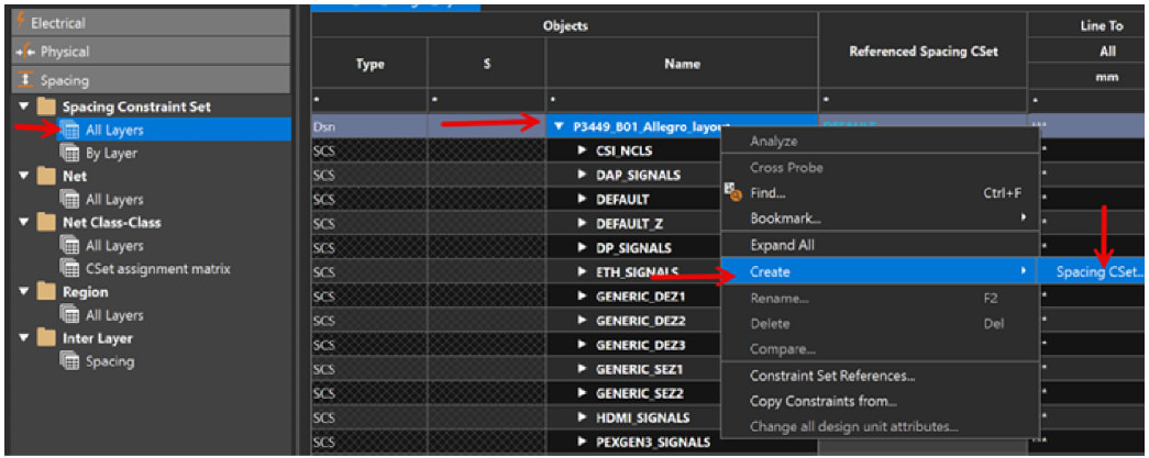
How to create a Spacing CSet in OrCAD X. For more detailed information, see the OrCAD X Constraint Management Guide.
Creating PCB Design Constraints for Spacing
Spacing constraints define clearances between objects like traces, pads, and vias.
Steps:
-
Navigate to the Spacing - Net > All Layers section in CM.
-
Group related nets into Net Groups:
-
Right-click selected nets and choose Create > Net Group.
Define a Spacing Constraint Set (SCS):
-
Go to Spacing Constraints Set - All Layers.
-
Specify minimum clearance between:
-
Trace-to-trace or trace-to-via.
Define a Spacing Constraint Set (SCS):
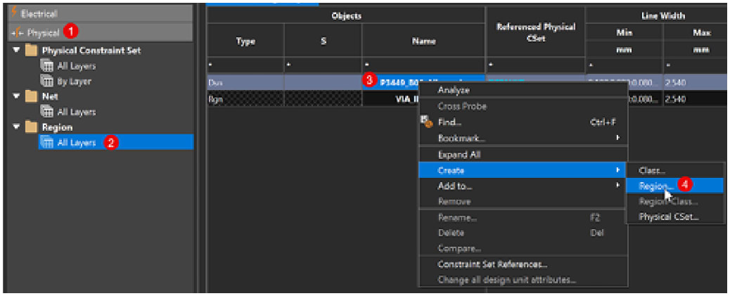
How to create a new constraint region in OrCAD X. For more detailed information, see the OrCAD X Constraint Management Guide.
Creating Constraint Regions
Constraint regions allow area-specific rules, such as tighter spacing under a BGA.
Steps:
-
In CM, go to Physical or Spacing - Region > All Layers.
-
Create a new region:
-
Right-click the worksheet and select Create > Region.
Define a Constraint Set for the region:
-
Example: Set minimum trace width to 4 mils under the BGA.
Apply the CSet to the region.
Applying the Region in PCB Layout:
-
In OrCAD X Presto PCB Editor, use Add Shape to draw the region.
-
Assign the Region Rules in the Properties panel.
Creating PCB design constraints is crucial to ensure your board is well-designed and manufacturable. With OrCAD X, engineers can easily create and manage electrical, physical, and spacing rules using tools like Net Classes and Regions. Explore how Cadence's PCB Design and Analysis Software and OrCAD X platform streamline constraint setup and ensure reliable PCB performance.
Leading electronics providers rely on Cadence products to optimize power, space, and energy needs for a wide variety of market applications. To learn more about our innovative solutions, talk to our team of experts or subscribe to our YouTube channel.