How to Generate Gerber Files in OrCAD X
Key Takeaways
-
Gerber file artwork is the layer-by-layer information of the design that makes review and adjustment easier for fabrication processes.
-
OrCAD X users can easily adjust the view settings to prepare Gerber file artwork.
-
Designers can review and confirm their design by outputting Gerber file artwork into a PDF.
OrCAD X users can customize Gerber file output in the Artwork Control Form.
Gerber files are artworks or images, a visual map for each layer of your layout. They are a critical layout output that guides fabrication for the CAM operator, allowing them to view board layers individually to account for manufacturing processes. The most pertinent questions when generating Gerber files are what views the artwork needs to capture and how to accomplish the task. Designers new to design for manufacturing (DFM) outputs who are wondering how to generate Gerber files in OrCAD X need look no further than this short walkthrough.
Generating Gerber Files in OrCAD X
|
Common Extensions |
Function/layer |
|
.AST .GTP / .SPT .GTO / .SST .GTS / .SMT .GTL / .TOP .IN1 .IN2 .INX .PWR .GND .GBL / .BOT .GBS / .SMB .GBO / .SSB .GBP / .SPB .ASB .GKO / .GKL / .DRD .DRL / .TXT / .TAP |
Top-side assembly Top-side solder paste Top-side silkscreen Top-side soldermask Top layer First inner layer (routing/plane) Second inner layer (routing/plane) Nth inner layer (routing/plane) Power plane layer Ground plane layer Bottom layer Bottom-side soldermask Bottom-side silkscreen Bottom-side solder paste Bottom-side assembly Board outline / mechanical Drilling information |
Understanding How to Generate Gerber Files in OrCAD X
As mentioned, Gerber files give the CAM operator a slice-by-slice view of the board; since the design is “static” at the time of manufacturing output, operators can more thoroughly investigate layers one at a time before sending their outputs to the fabricator. Individual Gerber files include all the information relevant to one layer, e.g., the artwork for the top layer has all the copper features on the board’s top side. Some design elements, like through-holes, can appear on multiple layers, reflecting their presence across the z-axis of the stackup.
Gerber artwork must then capture all relevant layers in the canvas view to convey all critical information to the CAM operator. After toggling the pertinent layers of the canvas view, users will want to save the Film settings by following these straightforward steps:
-
From the canvas view, select Manufacturing, then Export to Manufacturing from the top navbar. This will open the Exportsmenu.
-
In the Gerber dropdown (default name is Fabrication_Gerber), users can toggle the layers for output from the following list:
-
External Conductor
-
Internal Conductor
-
Internal Plane
-
Internal Negative Plane
-
Silkscreen
-
Soldermask
-
Solderpaste
-
Fabrication Drill Views
-
Assembly Drawing Views
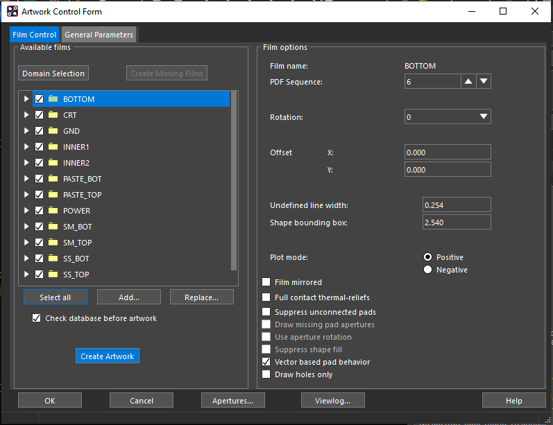
Users can edit the subclasses that appear on each layer by clicking the Configure Artwork Films button in the bottom-left corner.
-
-
After finalizing the films’ subclasses, users can output the Gerber files by clicking the Export button in the bottom-right corner of the Exports menu.

Inner layer Gerber artwork shown in PDF
What Subclasses Should My Films Include?
Designs must change their subclass layers within the films to accommodate specific design factors. However, most “standard” designs can use a simple 6-layer stackup template for films and subclasses.
|
Film |
Subclass(es) |
|
|
Cadence Solutions for Manufacturing Outputs
Designers wondering how to generate Gerber files (or other manufacturing files) can create them with the straightforward and easy-to-use UI of OrCAD X. Within the new OrCAD X platform, customizing file parameters prior to output is a cinch, whether that’s drill charts, mechanical outlines, test points, pick-and-place data, and more. Interested in seeing all OrCAD X has to offer for simulation, design, and documentation? Cadence’s PCB Design and Analysis Software page gives design teams all the tools they need to meet the challenges of modern electronic development cycles.
Leading electronics providers rely on Cadence products to optimize power, space, and energy needs for a wide variety of market applications. To learn more about our innovative solutions, talk to our team of experts or subscribe to our YouTube channel.