Home
Free Trial
Home
Free Trial
Read More
Content
Filter
10 results found
Featured
ICT vs Flying Probe: Factory Testing of PCB Assemblies
Featured
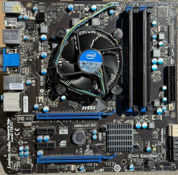
Printed Circuit Board Design For Assembly
Featured
Printed Circuit Board Design for Test
Featured
Testing Printed Circuit Boards and Assemblies
Featured
Printed Circuit Board Design for Manufacturing
Featured
A Guide to PCB Connectors: Selection, Design, and DFM Tips
Featured
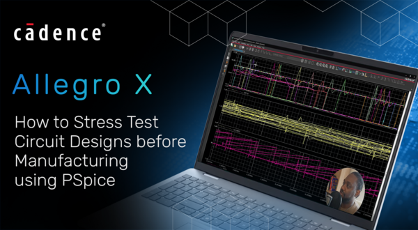
How to Stress Test Circuit Designs before Manufacturing using PSpice
Featured
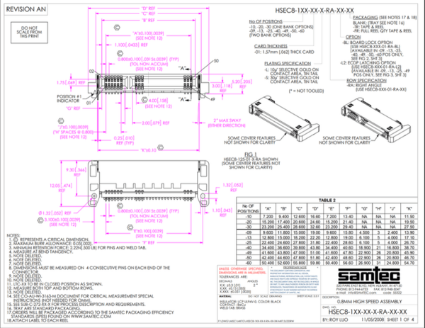
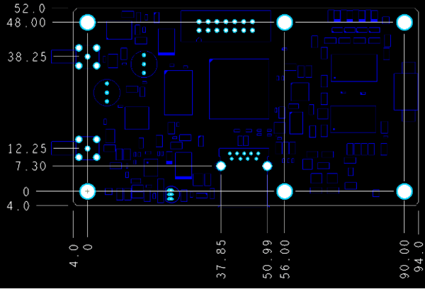
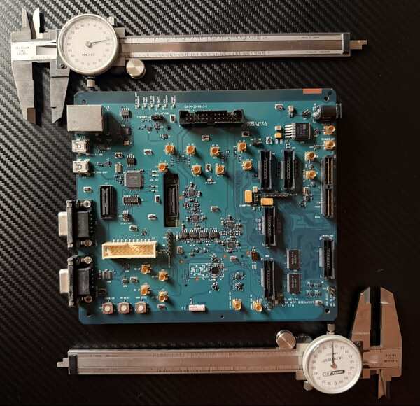
Tolerances and Dimensions Pertaining to PCB Fabrication
Featured
Inspecting Printed Circuit Boards and Assemblies
Featured
Flex Circuit Design Practices For Manufacturing and Assembly
Featured
Products
None
Allegro X PCB
(3)
Content types
None
Blog
(9)
Video
(1)
Solutions
None
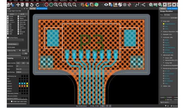
PCB Layout
(7)