Using an Electronic Component Footprint Library with OrCAD X
Key Takeaways
-
Organized footprint libraries ensure accurate component placement and reduce errors in PCB design.
-
OrCAD X integrates with SamacSys, Ultra Librarian, and SnapEDA for instant access to millions of components.
-
The OrCAD X footprint wizard simplifies footprint creation, ensuring compliance with industry standards.
OrCAD X electronic component footprint library from online providers.
An easily accessible electronic component footprint library can make your PCB layout workflow much more streamlined. These libraries contain standardized outlines, pad configurations, and dimensional information required to make sure you can mount your component to the board during the assembly stage.
A robust footprint library not only streamlines the design process but also reduces errors during the manufacturing phase. This article begins by exploring the fundamental concepts behind electronic component footprints and associated libraries, in addition to explaining how OrCAD X can aid in this workflow.
Comparison of Electronic Component Footprint Library Types
|
Library Type |
Description |
Advantages |
Disadvantages |
|
User |
Personal libraries where designers store component footprints, board outlines, and design data. |
Fast, efficient, and fully controlled by the individual designer. |
Lacks quality tracking and version control; changes can go unnoticed and may corrupt data if multiple users have access. |
|
Project |
Libraries organized by projects, often including project-specific data like varying footprint sizes and layer stackups. |
Enables selection of the correct part version for specific designs, accommodating different manufacturing methods. |
Requires careful monitoring by a CAD librarian; risk of designers selecting the wrong footprint. |
|
Corporate |
The master library is maintained by the company, with rigorous validation and controlled access. |
Ensures accurate, up-to-date footprints with robust quality control. |
Limited user access and strict restrictions can slow down the design process. |
Each footprint includes details such as pad layout, spacing, and orientation—critical parameters that ensure proper alignment and solderability on a PCB. These libraries are often developed in accordance with industry standards and manufacturer recommendations, ensuring compatibility across different platforms and processes.
Key Considerations for Designers Working with Footprint Libraries
Finding associated footprints for common components is usually straightforward, especially for standardized ICs and components with predefined package formats. Many libraries contain footprints for these common packaging formats.
However, when working with a new component without a predefined footprint, ensure it accurately reflects the component’s physical characteristics, including:
-
pin pitch,
-
pad size,
-
and overall dimensions.
Make sure to cross-reference multiple sources such as the component datasheet. Additionally, using advanced PCB software like OrCAD X, which includes a footprint wizard, can greatly simplify the process.
The OrCAD X Footprint Wizard
OrCAD X offers an advanced footprint wizard to simplify the creation and editing of footprints. The wizard assists with defining pad geometries, pin pitches, and overall component dimensions, ensuring compliance with manufacturing standards.
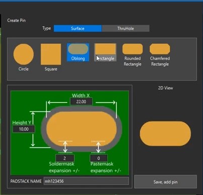
Screenshot of OrCAD X footprint wizard
Working with an Electronic Component Footprint Library in OrCAD X
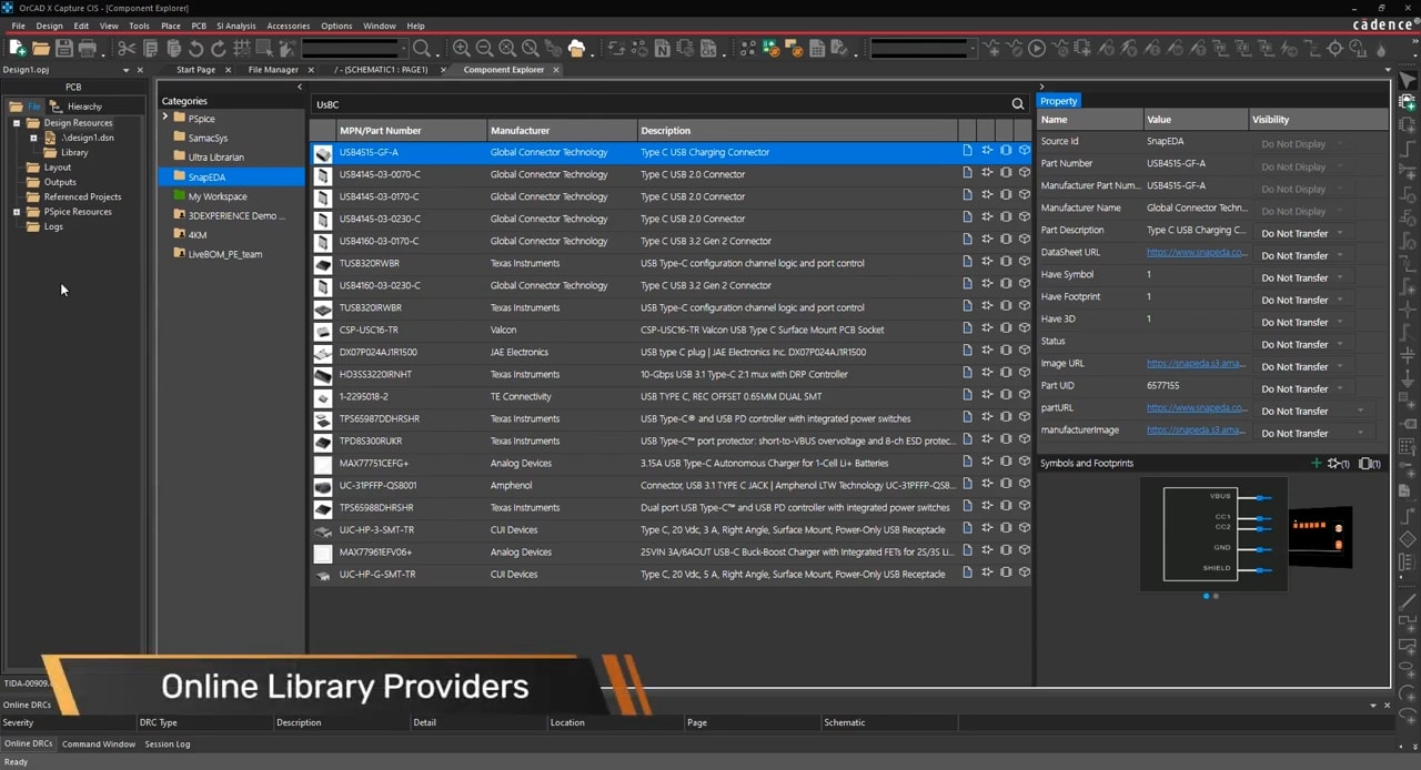
OrCAD X integrates seamlessly with three online library content providers giving you access to millions of components at the tip of your fingers. These content providers are SamacSys, Ultra Librarian and SnapEDA. You’ll be able to instantly use millions of pre-built component footprints and schematic symbols. This integration allows designers to quickly search for and download the latest part data without leaving the design environment.
Adding an Electronic Component Footprint to Your Library in OrCAD X
-
Initiate Online Component Placement: Click on Place > Component within OrCAD X Capture. This will open the integrated Component Explorer search interface.
-
Perform a Universal Search: In the search field, type the name or keyword of the component you need (e.g., "usb-c connector"). The search will query all integrated library content providers—SamacSys, Ultra Librarian, and SnapEDA.
-
Review Search Results: The results will display multiple entries that include datasheets, schematic symbols, PCB footprints, and even 3D models. Browse through the list to compare options.
-
Inspect Component Details: Select a component to open its property panel. Here, you can view detailed information, such as:
-
Datasheet links
-
Previews of the schematic symbol and PCB footprint
-
Part metadata
-
Add the Component to Your Schematic: Once you find the component that meets your requirements, double-click it or click the plus (+) sign next to Symbols and Footprints in the Property panel. This action will download the schematic symbol and PCB footprint into your local design directory.
-
Integrate into Your Library (Optional): You can also choose to add the component to your personal library or link it to an existing part. This option imports all relevant parametric data, ensuring that your library remains up to date.
Enhanced Navigation and Search
OrCAD X footprint libraries are equipped with search capabilities such as filtering by attributes like footprint name, size, or package type, making it easy to sift through extensive libraries. Additionally, the intuitive library tree and preview functionality allow designers to quickly inspect component details before placement, ensuring that each selected footprint meets the required specifications. This level of granularity enhances productivity and minimizes the likelihood of selecting incorrect parts.
Cloud & Local Flexibility
One of the key strengths of OrCAD X is its flexibility in managing libraries. Designers can opt for locally stored libraries for rapid access and minimal latency during design tasks. Alternatively, cloud-connected libraries offer centralized management, version control, change history, and collaboration, which is especially beneficial for large teams working on multiple projects. The cloud option provides real-time updates and ensures consistency across the organization, while local libraries allow individual designers to work independently when needed. This dual approach accommodates diverse workflows and organizational requirements, ensuring optimal efficiency and control throughout the design process.
An efficient electronic component footprint library reduces design errors and speeds up PCB development. OrCAD X offers powerful footprint management tools, including a footprint wizard and integration with major online libraries. Explore more on the Cadence PCB Design and Analysis Software page and learn more about the OrCAD X platform.
Leading electronics providers rely on Cadence products to optimize power, space, and energy needs for a wide variety of market applications. To learn more about our innovative solutions, talk to our team of experts or subscribe to our YouTube channel.