PCB Routing Tolerances and PCB Flatness Tolerance Standards
Key Takeaways
-
PCB flatness tolerance affects assembly, soldering, and mechanical stress, ensuring reliable performance.
-
PCB routing tolerance includes trace width, clearance, and spacing rules, critical for manufacturability and signal integrity.
-
OrCAD X Constraint Manager allows designers to define and enforce routing and flatness tolerances for optimal PCB performance.
The flatness of a PCB can refer to its twist/ bow, or the flatness of its layers.
PCB flatness tolerance refers to the allowable deviation from a perfectly flat surface, ensuring that the PCB can be properly assembled and function correctly in its final application. A flat PCB ensures accurate component placement, which is essential for proper soldering and electrical connections.
PCB routing tolerance refers to the allowable variations in trace width, spacing, and clearance that ensure reliable signal integrity and manufacturability. These tolerances help maintain consistent electrical performance while preventing issues like crosstalk and short circuits.
Read on as we cover PCB flatness standards and how to define PCB routing tolerances in OrCAD X that meet industry standards and fabrication requirements.
PCB Flatness-Related Standards
|
Standard |
Description |
Key Flatness Tolerances |
|
IPC-6012 |
|
Class 1: Cosmetic imperfections allowed. Class 2: High performance, extended life, minor imperfections allowed. Class 3: Critical applications, minimal imperfections allowed. |
|
IPC-A-600 |
|
Bow and twist tolerances: SMT applications - ≤0.75% of diagonal length, Non-SMT applications - ≤1.5% of diagonal length. |
|
IPC-9641 |
|
Focuses on warpage control during thermal cycles, especially reflow soldering. |
PCB Flatness Tolerance In Terms of Bow and Twist
Flatness in PCBs is assessed by two characteristics: bow and twist.
-
Bow is characterized by a cylindrical or spherical curvature, with all four corners of the board remaining in the same plane.
-
Twist refers to deformation along the board's diagonal, causing one corner to be out of plane with the other three.
Bow and twist can be affected by the board design, circuit configurations, and multilayer constructions, which introduce different stress conditions. Material properties and board thickness also play a role in flatness. Bow and twist are measured and calculated as a percentage according to IPC-TM-650 – 2.4.22.
The acceptable limits for bow and twist are:
-
For printed boards with surface mount components: 0.75% or less.
-
For all other boards: 1.5% or less.
Thickness and Tolerance
For standard PCBs that are 31 mils or thicker, the thickness tolerance is typically ±10%. This means that a board specified to be 62 mils thick could actually measure between 55.8 mils and 68.2 mils and still be within acceptable limits. For thinner boards (less than 31 mils), the tolerance is tighter, at ±3 mils. Thus, a board specified to be 20 mils thick could measure between 17 mils and 23 mils.
Advanced PCB Thickness Tolerance
For more demanding applications, especially where precise control of impedance and other electrical properties is required, advanced PCBs might have tighter thickness tolerances. These could be as precise as ±5%. The thickness tolerance is crucial because it directly affects the electrical properties of the PCB, such as impedance, capacitance, and inductance. Variations in thickness can lead to variations in these properties, which can affect the performance of high-frequency and high-speed circuits.
Staying Within Tolerance With OrCAD X
|
Design Consideration |
Description |
Best Practices |
Associated OrCAD X Features |
|
Balanced Copper Distribution |
Ensuring even copper distribution across the PCB to prevent differential expansion and contraction. |
|
Easily create and manage copper pours and shapes, including automatic adjustments for components and traces. |
|
Symmetrical Layer Stack-up |
Designing the PCB stack-up symmetrically to maintain even stress distribution during thermal cycling. |
|
Set up and visualize different stack-ups, ensuring symmetrical layer design and consistent dielectric thickness with the cross section editor. |
|
Controlled Impedance Design |
Designing for controlled impedance to maintain electrical performance while ensuring mechanical stability. |
|
Set up and enforce impedance control and other electrical constraints to ensure signal integrity with the constraint manager options. |
|
Thermal Management |
Incorporating thermal management strategies to minimize warpage due to temperature changes. |
|
OrCAD X offers tools to automatically generate thermal reliefs, visualize thermal distribution and manage heat sinks, spreaders, thermal vias, and thermal relief patterns. |
|
Mechanical Considerations |
Designing for mechanical robustness to maintain flatness during and after manufacturing. |
|
Integrate 3D models to ensure mechanical robustness and proper fit within enclosures. DFM Checks: Perform design for manufacturability checks to ensure mechanical reliability. |
PCB Routing Tolerance With OrCAD X Constraint Manager
The OrCAD X Constraint Manager lets you define, manage, and apply a variety of PCB routing tolerances throughout your PCB project. It organizes constraints into several domains—typically physical, electrical, and spacing—so you can precisely control how your board is routed and ensure your design meets both manufacturing and signal integrity requirements.
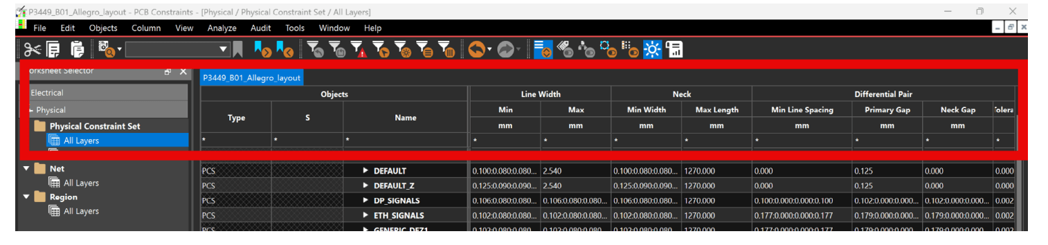
Setting Up Physical Constraints and Tolerances
Physical constraint sets specify the PCB routing tolerances related to the geometry of your routing. These include minimum and maximum trace widths, neck widths (the narrow portions allowed in traces), and maximum neck lengths. They can also control which vias (or other routing features) are allowed for certain nets.
-
Open the Constraint Manager: In the PCB editor (or even from OrCAD X Capture when using the integrated flow), navigate to the “Physical” section.
-
Create a New CSet: Right-click in the worksheet and choose to create a new Physical CSet. For example, you might name one “POWER_GND” and set tolerances such as:
-
Minimum line width (e.g., 0.381-mm)
-
Minimum neck width (e.g., 0.127-mm)
-
Maximum neck length (e.g., 5.08-mm)
Assign CSet to Nets: Once created, these physical rules can be applied globally or to specific nets. For instance, you might assign the “POWER_GND” set to all power and ground nets to ensure they are routed with thicker traces and stricter spacing rules.
PCB Routing Tolerance for Differential Pairs
-
For differential pairs, you might create a separate physical constraint set (e.g., “DP”) with rules that specify the trace width and primary gap (the spacing between the two traces of the differential pair).
-
This ensures that both lines in the pair are consistent and within tolerance for high-speed signaling.
Defining Electrical Constraints and Tolerances
In the electrical domain, you can set rules for differential pairs to ensure proper PCB routing tolerances for signal timing and phase control. These rules include parameters like:
-
Gather Control: Determines whether the routing should “couple” (bring the traces together) or “ignore” coupling until later in the routing process.
-
Uncoupled Length: Specifies how much of the route can be uncoupled before the differential pair must be brought back into alignment.
How to Set Electrical Constraint Rules:
-
In the Constraint Manager’s Electrical section (often under a “Routing” worksheet), you can create an Electrical CSet for differential pairs and then set the desired values for parameters such as gather control and phase tolerances.
-
Once these are defined, you assign the Electrical CSet to the nets that are part of your differential pair (or even to a net group that contains all differential pair nets).
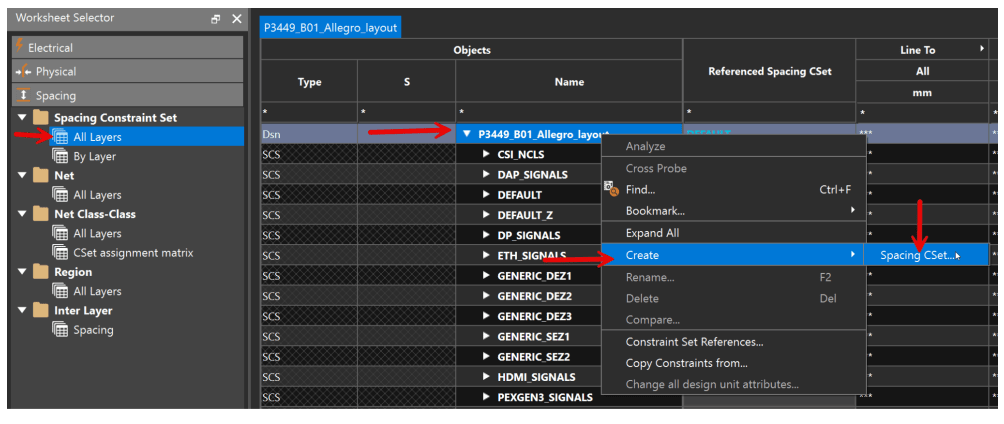
Setting Up Spacing Constraints (Clearance Tolerances)
Spacing constraints set the minimum distance (clearance) required between different conductive elements—such as between traces, pads, vias, and other features. These provide another method of PCB routing tolerances for avoiding shorts, ensuring proper isolation, and maintaining signal integrity.
-
Create a New Spacing CSet: Within the “Spacing” section of the Constraint Manager, right-click to create a new spacing set. For example, for USB signals or high-voltage nets, you might create a set called “SCS_USB” that specifies a clearance of 10-mils (0.254-mm) between objects.
-
Apply to Net Groups: Often, you will have groups of nets that share common spacing requirements (like all nets for a USB interface). The Constraint Manager allows you to create net groups and then apply the spacing rules to the entire group in one step.
Managing PCB routing tolerance and PCB flatness tolerance is key for good PCB design. OrCAD X provides a stackup editor and constraint management tools to define, enforce, and verify design tolerances, ensuring compliance with industry standards. Learn more about Cadence’s PCB Design and Analysis Software and OrCAD X to streamline your PCB development process.
Leading electronics providers rely on Cadence products to optimize power, space, and energy needs for a wide variety of market applications. To learn more about our innovative solutions, talk to our team of experts or subscribe to our YouTube channel.