Navigating Signal Integrity Challenges in High-Speed PCB Design: Practical Tips to Solve Common Obstacles

If you're anything like me, you've probably faced the headaches that come with signal integrity (SI) issues in high-speed PCB design. That nagging problem shows up just when you think your layout is solid - unexpected reflections, data errors, or noisy signals that won't behave no matter what you try. Trust me, I've been there. Over the years, I've learned that while SI can seem like a complex beast, many common obstacles have practical solutions that you can apply with the right mindset and tools.
Let's talk through some typical signal integrity problems I've encountered and, more importantly, how I tackle them in my designs. Hopefully, by the end of this, you'll feel a bit more confident when SI challenges come knocking on your door.
Common Signal Integrity Obstacles and Why They Happen
First, what are we dealing with when we say "signal integrity"? In simple terms, it's about ensuring signals traveling through your PCB traces arrive cleanly and without distortion. But the reality is that fast signals can behave unpredictably, and several issues tend to pop up regularly.
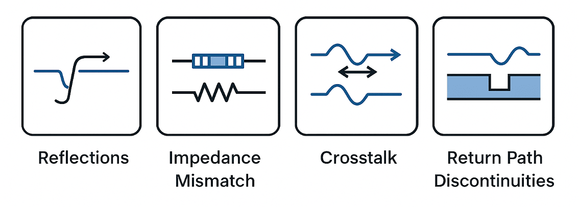
For me, the most common culprits are:
- Reflections: Ever hear an echo when you shout in a canyon? That's basically what happens inside your PCB traces when the impedance isn't matched. A signal hits a discontinuity, like an open-ended trace or an improper termination, and part of it bounces back.
- Impedance mismatch: If your trace impedance doesn't match the source and load, signals can reflect, slow down, or degrade. Getting controlled impedance right is critical, especially with high-speed differential pairs.
- Crosstalk: This happens when signals on adjacent traces interfere with each other. Think of it like two people talking loudly in adjacent rooms; one voice can bleed over and cause confusion.
Return path discontinuities: The signal's return path isn't always obvious but essential. Interruptions in the ground or power planes force return currents to find longer, unwanted paths, creating noise and EMI issues.
I recall a design a few years ago in which intermittent failures were traced back to a combination of poorly routed differential pairs and a missing ground plane layer. Solving those issues was a frustrating journey, but it taught me valuable lessons I still use today.
How I Diagnose Signal Integrity Problems Step-by-Step
Before pursuing solutions, I always remind myself that you can't fix what you don't understand. That means measurement and simulation are your best friends.
Here's how I usually approach diagnosing SI issues:
- Review the stackup and materials: I double-check the PCB stackup layers, dielectric constants, and trace widths. Even minor changes in materials affect impedance.
- Verify impedance control: Using my CAD tools, I validate that the trace impedance matches the design targets, which are usually 50 ohms single-ended or 90 ohms differential. Tools like Cadence Sigrity make this easier than ever.
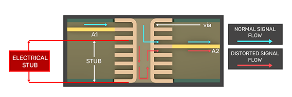
- Check routing topology: I look for unnecessary stubs, sharp bends, or vias that might cause reflections or signal loss. Often, cleaning up routing can solve half the problem.
- Inspect return path integrity: I ensure continuous reference planes under high-speed traces to maintain low inductance return paths. If there's a gap in the ground plane, I know it's a red flag.
- Simulate critical nets: I run time-domain reflectometry (TDR) or eye-diagram simulations using Cadence Sigrity Aurora PCB Analysis tools to predict issues before manufacturing.
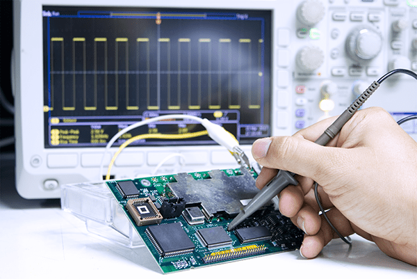
Suppose you don't have access to advanced simulators. In that case, I find that building a simple test fixture or using a high-bandwidth oscilloscope to measure signal waveforms on the prototype can reveal a lot.
Practical Techniques I Use to Improve Signal Integrity
Once I have a clear picture of the problem, here are the techniques I consistently apply to get signals back on track:
- Controlled impedance routing: I stick to precise trace widths and spacing as defined by the stackup. I maintain constant spacing and length matching for differential pairs to minimize skew and noise.
- Avoiding stubs and vias: Whenever possible, I keep traces direct and minimize the number of vias. Each via adds inductance and potential reflection points. If vias are unavoidable, I ensure they are properly modeled in simulations.
- Proper termination: I use the right termination scheme depending on the interface, whether it's a transmission line, CMOS, or LVDS. For example, series termination resistors close to the driver can significantly reduce reflections.
- Ground and power plane design: I pay special attention to continuous, unbroken ground and power planes. They provide clean reference planes that reduce return path impedance and lower EMI.
- Strategic decoupling capacitors: Placing decoupling capacitors close to power pins helps suppress noise and stabilize the power distribution network.
I remember a challenging design where applying these best practices, especially improving ground plane continuity and adding the right termination, can drastically improve signal quality. The project went from unpredictable failures to a clean, stable operation that passed all tests with margin.
Looking Ahead: Emerging Trends in Signal Integrity
As data rates climb beyond 10 Gbps and new signaling methods like PAM4 emerge, signal integrity challenges only grow more complex. 3D IC packaging and advanced materials add layers of nuance to PCB design.
My advice is to keep learning and leverage simulation tools early and often in your design process. The more you understand your signals and their environment, the fewer surprises you'll face in the lab.
Wrapping Up
Signal integrity can feel daunting at first, but with a structured approach and practical techniques, it becomes manageable and even predictable. Whether it's verifying impedance, cleaning up routing, or ensuring solid return paths, these steps help you deliver robust, high-speed designs your colleagues will appreciate.
If you ever find yourself stuck, don't hesitate to revisit the basics and apply these tried-and-true methods. And of course, the Cadence toolset offers powerful capabilities to make your life easier every step of the way.