Grounding and Return Paths: Power Plane No-Nos
Why Grounding Still Trips Up Designers
Grounding is one of the oldest principles in electronics, yet it continues to cause trouble for even the most seasoned PCB designers. It is easy to assume that ground simply means a big copper pour or a reference net that takes care of itself. But in high-speed digital and mixed-signal designs, this assumption can lead to serious issues that are often difficult to diagnose.
When engineers overlook how return currents actually flow, they risk creating noisy systems, failed EMI tests, and signal integrity problems that appear only when the board is under load. These are not just theoretical risks. Poor grounding and disconnected return paths show up as timing glitches, data corruption, or strange power rail behavior that can be expensive to debug and fix after manufacturing.
The truth is, grounding is not just about where you place your GND nets. It is about how signals return, how layers interact, and how your layout supports stable, predictable behavior across all operating conditions. As designs become faster and denser, grounding requires more deliberate planning.
This article is for engineers who want to avoid common pitfalls, understand real return path behavior, and use the tools available to build more reliable boards from the start.
Return Path Basics: What You Can't Ignore
Every signal that travels through a trace on a PCB has a return current that flows back to its source. This concept is simple, but in practice, it is often misunderstood or overlooked. Many layout issues that appear as signal integrity or EMI problems are actually caused by poor return path planning.
The return path does not take the shortest distance back. It takes the path of least impedance, which usually means following directly under the signal trace when a solid ground plane is present. This tight coupling between signal and return minimizes loop area, which is critical for reducing both radiated emissions and susceptibility to external noise.
Problems arise when signals change reference planes without proper stitching vias or when split planes interrupt the return current. In these cases, the current is forced to detour, often creating a large loop that increases inductance, adds noise, and degrades signal quality. In differential pairs, imbalanced return paths can destroy timing and create cross-domain interference.
The key is to visualize every signal and its return path as a complete, closed loop circuit. For high-speed and sensitive signals, maintaining a continuous, low impedance return path is just as critical as controlling trace impedance. Any interruption, such as a plane split, via transition without adjacent ground stitching, or sudden layer change, can introduce discontinuities that degrade signal integrity or increase EMI.. Ensuring return path continuity and impedance control during layout is essential for maintaining signal integrity, especially in high-speed or mixed-signal designs. This process can be supported through constraint-driven design environments like Allegro X, which allow engineers to assess these factors directly during PCB layout and catch issues before fabrication.
By respecting the return path as much as the forward path, you can avoid many of the pitfalls that lead to unstable or noisy systems, especially in high-speed designs.
Power Plane Pitfalls: What Not to Do
Power planes are essential for delivering low-impedance current to components, but if they are poorly designed, they can become one of the main sources of signal integrity and EMI issues. A common mistake is assuming that a large copper pour automatically equals a good power delivery network. In reality, it is how that copper is structured and connected that makes the difference.
One of the biggest errors designers make is splitting power or ground planes without understanding the consequences. For example, placing a high-speed signal trace over a split or void in the reference plane forces the return current to find an alternate path, often across a longer or higher impedance route. This breaks the controlled impedance of the signal and creates EMI hotspots.
Another common issue is using long power stubs that connect components far away from the bulk of the power plane. These stubs act like antennas, radiating high-frequency noise and contributing to power rail instability. Similarly, islands of copper that are not properly tied to the main plane through stitching vias can become floating nodes that introduce unpredictable behavior.
Good power plane design involves continuous, unbroken planes that provide a stable reference for signals and a low-impedance path for current. Every signal layer should have a solid reference plane directly adjacent to it, and power planes should be carefully managed to avoid unnecessary segmentation.
Allegro X enables early identification of layout issues by combining constraint-driven design with dynamic plane shaping. These capabilities allow engineers to create power planes that maintain signal integrity by supporting well-defined return paths and consistent impedance. When applied correctly, the power distribution network functions as an integral part of the design rather than a potential source of electromagnetic or timing problems.
Stitching Vias and Ground Plane Integrity
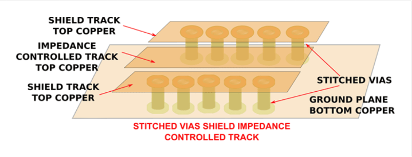
Image Credit: PCB Trace - What is Via Stitching and Why it is Useful
A solid ground plane is not just a design checkbox, it is the foundation of signal stability and low-noise performance. But even the best-designed planes lose effectiveness without proper vertical connectivity- this is where stitching vias come in.
Stitching vias are vertical connections between ground or power planes on different layers of the PCB. Their purpose is to maintain return path continuity when signals transition between layers, especially during high-speed routing. Without them, return currents can be forced into convoluted paths that increase loop area and inject unwanted noise into the system.
Another overlooked benefit of stitching vias is their role in reducing EMI. By tightly coupling signal and return paths through multiple layers, stitching vias prevent return currents from straying into unshielded areas. This minimizes radiation and improves the board chances of passing EMI compliance on the first try.
Some designers rely heavily on copper pours to extend their ground reference, but wide pours are not a substitute for a well-connected plane. A pour without adequate vias is just a disconnected island. Solid planes-especially when stitched properly-provide a lower impedance path and far better thermal and electrical performance.
Cadence Allegro X helps enforce these design rules automatically. You can define via spacing constraints, visualize return path continuity, and ensure your ground plane is doing its job across the entire board. In high-speed layouts, good grounding is not just about the surface-it is about building a three-dimensional shield that supports every signal from top to bottom.
Mixed-Signal Layouts and Return Path Isolation
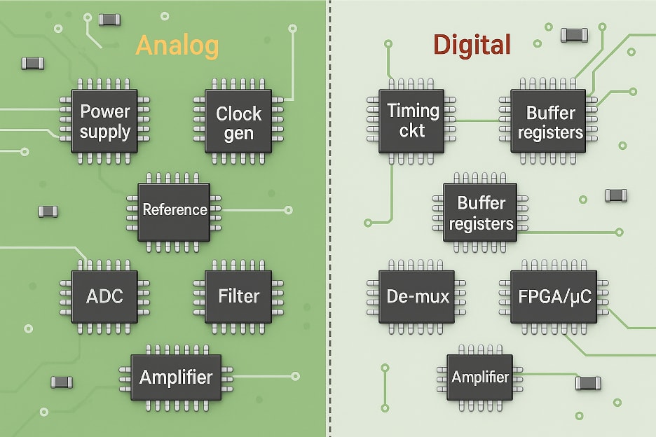
Designing PCBs that include both analog and digital circuits presents a unique challenge: keeping noise-sensitive signals protected without compromising return path integrity. The solution is not just to separate analog and digital grounds. It is to manage how those grounds interact under real operating conditions.
In many cases, designers are told to split the ground plane between analog and digital regions. While this sounds like good isolation on paper, it often introduces more problems than it solves. When a digital signal crosses the gap between these planes, its return current cannot follow. Instead, it detours around the split, creating a large loop area that increases EMI and can degrade analog performance.
A more effective approach is to maintain a continuous ground plane and isolate noise through layout zoning, filtering, and controlled return paths. In some systems, however, strong digital switching noise may interfere with sensitive analog circuitry, prompting the need for partial ground separation. When this is necessary, it is important to preserve a predictable return current path by creating a controlled connection point between the analog and digital grounds. This can be done using single-point grounding, carefully placed stitching capacitors, or ferrite beads that block high-frequency noise while allowing low-frequency return currents to flow. These techniques help prevent the formation of large loop areas and reduce the risk of coupling. Simulation tools like Cadence Sigrity are valuable in these scenarios because they allow designers to visualize current flow and confirm that return paths remain intact across domains.
With the right grounding and layout strategy, analog precision and digital speed can coexist on the same board without compromise. The goal is not to divide your board with barriers, but to guide your currents with clarity.
Best Practices: Designing with Return Paths in Mind
Great PCB layouts start with a clear understanding of current flow. For every signal you route, a corresponding return current must travel a complementary path. When this path is broken, rerouted, or ignored, problems begin to stack up quickly. That is why return path planning should begin before a single trace is drawn.
The most effective way to maintain clean return paths is to assign solid reference planes directly beneath each signal layer. This keeps return currents tightly coupled to their signals, minimizes loop area, and improves both signal integrity and EMI performance. Avoid routing over voids, plane splits, or component gaps that disrupt this relationship.
When signals change layers, add stitching vias near the transition points to keep return currents close. Plan your stackup to pair signal layers with adjacent ground or power planes, and always double-check that those planes are continuous. Floating copper shapes may look helpful but can introduce more confusion than benefit if they are not tied in properly.
.Treating return paths as part of the signal path rather than an afterthought leads to more reliable and predictable designs that are easier to validate. Tools such as Allegro X support this approach, providing return path visualization, constraint-based routing, and real-time rule checking to help enforce these best practices during layout.