3D PCB Viewer Functionality With OrCAD X Free Viewer
Key Takeaways
-
A 3D viewer allows design review to evaluate the board in three-dimensional space, which can be relevant to manufacturing and placement concerns.
-
Reviewers can also better assuage the impact of signal integrity, EMI, or EMC placement and routing in three dimensions.
-
The OrCAD X Free Viewer is the perfect tool for design reviews of board files and schematics.
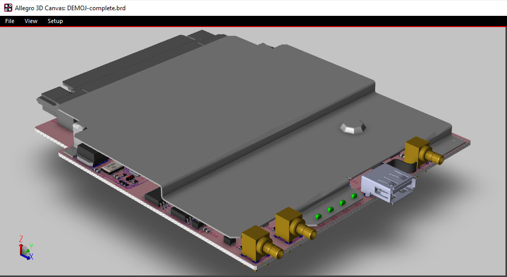
A 3D PCB viewer lets users manipulate the view of the board layout and improve manufacturing outcomes.
It can be easy to overlook the work of synchronizing enclosures to a PCB. What may seem a simple issue of fitting the enclosure around the board and its components (including connectors), additional mechanical factors like thermal routing/cooling and user ergonomics come into play. A 3D PCB viewer makes checking for MCAD-ECAD integration trivial, and with support for leading MCAD tools, OrCAD X improves post-layout design for the mechanical team.
3D PCB Viewer Features
|
Free Viewer |
OrCAD X Presto PCB Editor |
|
|
Standard 3D Viewing Angles |
✔ |
✔ |
|
Free Rotation 3D View |
✖ |
✔ |
|
Highlight Net Copper |
✔ |
✔ |
|
Flagged DRC Violations |
✖ |
✔ |
|
Air Gap Measurements |
✖ |
✔ |
|
Layer Transparency Sliders |
✖ |
✔ |
|
Cutting Planes |
✖ |
✔ |
Preparing for Manufacturing With a 3D PCB Viewer
The foremost advantage of 3D modeling for PCBs is the ability to visually confirm system integration (through off-board connector placement) and MCAD-ECAD meshing. Especially for consumer products where shrinking enclosures have reduced the amount of board area available for placement and routing, being able to inspect critical placements like connectors before manufacturing begins visually improves the maneuverability of design teams to resolve layout issues pre-production. With the appropriate 3D models, reviewers can also diagnose any potential manufacturing/technician issues:
-
Solder shadowing - When significantly shorter SMT components neighbor taller components (e.g., consider a chip package next to a vertical connector), the larger component can block solder flow during wave soldering to the shorter component in the wake of the wave’s travel. Poor solder flow during wave soldering can result in incomplete or poor-quality solder joints that imperil device reliability. If space and performance allow, consider moving these shorter components away from the taller components.
-
Manual soldering/rework - Certain components may not be suitable or are entirely incompatible with the manufacturer’s automated placement and soldering equipment. If manual soldering is necessary, provide additional space around these components and consider the height of nearby components that may impede the technician’s ability to manipulate the soldering iron effectively.
-
Flying probe/bed of nails testing - Manufacturers use one of these testing methods to determine bare board and in-circuit continuity. Component spacing around test points shouldn’t obstruct contact between the probe and pad.
A view of the layout is also necessary to gauge many aspects of the board's performance. While the schematic describes circuit connections logically, circuit layouts require optimal component placement and interconnect routing. This information is usually within the manufacturer’s datasheet under a suggested layout. Failing its inclusion within the datasheet, designers can follow general best practices regarding net-to-net spacing, isolating analog/digital ground, etc., to optimize performance. A 3D view of the board allows design reviewers to adequately consider all relevant EMI, EMC, and signal integrity concerns that can inhibit in-circuit performance while minimizing cost expenditures related to manufacturing or rework.
OrCAD X Presto PCB Editor users can unlock even greater 3D functionality. With the 3DX Canvas, users can precisely customize the view options of their 3D PCB model for team collaboration and manufacturing preparation:
-
Customizable cutting planes - Users can define any cutaway view with a ± 90° pitch and yaw angle for the x, y, and z-axes and an offset distance slider to move the plane location. The default cutting planes match the six standard viewing sides of the board, and users can combine multiple cuts for additional viewing options.
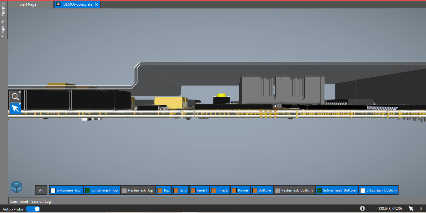
A cutaway of the board shows the internal via connections.
-
Layer transparencies - Like with the 2D board design, users can adjust the opacity of mechanical symbols or individual components to emphasize or deemphasize certain board features. They can toggle between full opacity, the global 3D model opacity set in the Display tab, or zero opacity (e.g., transparent). Users also have the option to suppress the model's visibility completely.
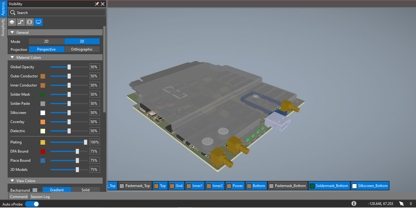
Users can adjust the opacity visibility settings in three dimensions.
-
3D DRC - Users can adjust the visibility of spacing violations (overlaps, spacing requirements, etc.) by changing the color, opacity, and toggling displayed/hidden elements of the DRC flags.
-
3D air gap measurements - By holding alt and selecting a board feature (pad, component, via barrel, track, plane), users will see a line displaying the shortest distance between the two objects.
Additional OrCAD X Free Viewer Capabilities
The OrCAD X Free Viewer has additional functionality that supports design reviews, too:
-
Footprint verification - Since the assembly's reliability depends on the footprint's accuracy to manufacturer specifications, design teams must incorporate a verification procedure to prevent PCBA production defects.
-
Cross-section report - Reviewers can see a breakdown of the stackup by material and thickness, including various electrical parameters like the dielectric constant, conductivity, and loss tangent that can accurately gauge real-world performance within an electromagnetic field solver.
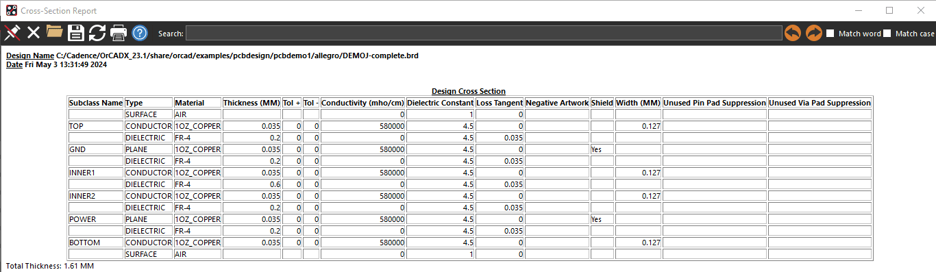
A Cross-Section Report gives reviewers basic information about the stackup.
-
Net coloring - Like cross-probing, reviewers can color nets to quickly identify critical signals like clocks and how the surrounding layout can influence or become influenced by them.
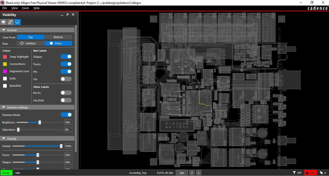
Viewer options, like brightness, saturation, and layer visibility, allow reviewers to highlight critical nets against the background design.
-
Capture Canvas - Reviewers can take a screenshot of their active canvas for internal communications, comments, and critique without operating various third-party screenshot tools.
-
Package review - Reviewers can inspect complex multi-die packages, including design features like wire bonds, silicon bridges, interposers, etc.
Cadence Solutions for All Levels of Design Team Experience
3D PCB viewers help design teams avoid potential manufacturing pitfalls that can slow down production and lead to revisions, which can be costly when projects are on strict budgets and deadlines. For users looking to expand their review capabilities, the OrCAD X Free Viewer provides schematic and layout review tools to jumpstart design pre-production. Interested in learning more about the new OrCAD X platform? Check out a free trial and see how Cadence PCB Design and Analysis Software can transform your projects.
Leading electronics providers rely on Cadence products to optimize power, space, and energy needs for a wide variety of market applications. To learn more about our innovative solutions, talk to our team of experts or subscribe to our YouTube channel.